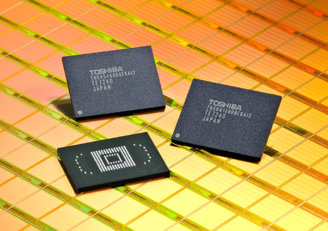
Understanding Flash: Blocks, Pages and Program / Erases

In the last post on this subject I described the invention of NAND flash and the way in which erase operations affect larger areas than write operations. Let’s have a look at this in more detail and see what actually happens. First of all, we need to know our way around the different entities on a flash chip (or “package“), which are: the die, the plane, the block and the page:

NAND Flash Die Layout (image courtesy of AnandTech)

NAND Flash Die Layout (image courtesy of AnandTech)

Note: What follows is a high-level description of the generic behaviour of flash. There are thousands of different NAND chips available, each potentially with slightly different instruction sets, block/page sizes, performance characteristics etc.

  • The package is the memory chip, i.e. the black rectangle with little electrical connectors sticking out of it. If you look at an SSD, a flash card or the internals of a flash array you will see many flash packages, each of which is produced by one of the big flash manufacturers: Toshiba, Samsung, Micron, Intel, SanDisk, SK Hynix. These are the only companies with the multi-billion dollar fabrication plants necessary to make NAND flash.
  • Each package contains one or more dies (for example one, two, or four). The die is the smallest unit that can independently execute commands or report status.
  • Each die contains one or more planes (usually one or two). Identical, concurrent operations can take place on each plane, although with some restrictions.
  • Each plane contains a number of blocks, which are the smallest unit that can be erased. Remember that, it’s really important.
  • Each block contains a number of pages, which are the smallest unit that can be programmed (i.e. written to).

The important bit here is that program operations (i.e. writes) take place to a page, which might typically be 8-16KB in size, while erase operations take place to a block, which might be 4-8MB in size. Since a block needs to be erased before it can be programmed again (*sort of, I’m generalising to make this easier), all of the pages in a block need to be candidates for erasure before this can happen.

Program / Erase Cycles

When your flash device arrives fresh from the vendor, all of the pages are “empty”. The first thing you will want to do, I’m sure, is write some data to them – which in the world of memory chips we call a program operation. As discussed, these program operations take place at the page level. You can then read your fresh data back out again with read operations, which also take place at the page level. [Having said that, the instruction to read a page places the data from that page in a memory register, so your reading process can in fact then selectively access subsets of the page if it desires – but maybe that’s going into too much detail…]

NAND-flash-blocks-pages-program-erasesWhere it gets interesting is if you want to update the data you just wrote. There is no update operation for flash, no undo or rewind mechanism for changing what is currently in place, just the erase operation. It’s a little bit like an etch-a-sketch, in that you can continue to turn the dials and make white sections of screen go black, but you cannot turn black sections of screen to white again without erasing the entire screen. Etch-a-SketchAn erase operation on a flash chip clears the data from all pages in the block, so if some of the other pages contain active data (stuff you want to keep) you either have to copy it elsewhere first or hold off from doing the erase.

In fact, that second option (don’t erase just yet) makes the most sense, because the blocks on a flash chip can only tolerate a limited number of program and erase options (known as the program erase cycle or PE cycle because for obvious reasons they follow each other in turn). If you were to erase the block every time you wanted to change the contents of a page, your flash would wear out very quickly.

So a far better alternative is to simply mark the old page (containing the unchanged data) as INVALID and then write the new, changed data to an empty page. All that is required now is a mechanism for pointing any subsequent access operations to the new page and a way of tracking invalid pages so that, at some point, they can be “recycled”.

NAND-flash-page-update

Updating a page in NAND flash. Note that the new page location does not need to be within the same block, or even the same flash die. It is shown in the same block here purely for ease of drawing.

This “mechanism” is known as the flash translation layer and it has responsibility for these tasks as well as a number of others. We’ll come back to it in subsequent posts because it is a real differentiator between flash products. For now though, think about the way the device is filling up with data. Although we’ve delayed issuing erase operations by cleverly moving data to different pages, at some point clearly there will be no empty pages left and erases will become essential. This is where the bad news comes in: it takes many times longer to perform an erase than it does to perform a read or program. And that clearly has consequences for performance if not managed correctly.

In the next post we’ll look at the differences in time taken to perform reads, programs and erases – which first requires looking at the different types of flash available: SLC, MLC and TLC…

caution[* Technical note: Ok so actually when a NAND flash page is empty it is all binary ones, e.g. 11111111. A program operation sets any bit with the value of 1 to 0, so for example 11111111 could become 11110000. This means that later on it is still possible to perform another program operation to set 11110000 to 00110000 for example. Until all bits are zero it’s technical possible to perform another program. But hey, that’s getting a bit too deep into the details for our requirements here, so just pretend you never read this…]

Advertisement

Understanding Flash: What Is NAND Flash?

circuit-board

In the early 1980s, before we ever had such wondrous things as cell phones, tablets or digital cameras, a scientist named Dr Fujio Masuoka was working for Toshiba in Japan on the limitations of EPROM and EEPROM chips. An EPROM (Erasable Programmable Read Only Memory) is a type of memory chip that, unlike RAM for example, does not lose its data when the power supply is lost – in the technical jargon it is non-volatile. It does this by storing data in “cells” comprising of floating-gate transistors. I could start talking about Fowler-Nordheim tunnelling and hot-carrier injection at this point, but I’m going to stop here in case one of us loses the will to live. (But if you are the sort of person who wants to know more though, I can highly recommend this page accompanied by some strong coffee.)

Anyway, EPROMs could have data loaded into them (known as programming), but this data could also be erased through the use of ultra-violet light so that new data could be written. This cycle of programming and erasing is known as the program erase cycle (or PE Cycle) and is important because it can only happen a limited number of times per device… but that’s a topic for another post. However, while the reprogrammable nature of EPROMS was useful in laboratories, it was not a solution for packaging into consumer electronics – after all, including an ultra-violet light source into a device would make it cumbersome and commercially non-viable.

US Patent US4531203: Semiconductor memory device and method for manufacturing the same

US Patent US4531203: Semiconductor memory device and method for manufacturing the same

A subsequent development, known as the EEPROM, could be erased through the application of an electric field, rather than through the use of light, which was clearly advantageous as this could now easily take place inside a packaged product. Unlike EPROMs, EEPROMs could also erase and program individual bytes rather than the entire chip. However, the EEPROMs came with a disadvantage too: every cell required at least two transistors instead of the single transistor required in an EPROM. In other words, they stored less data: they had lower density.

The Arrival of Flash

So EPROMs had better density while EEPROMs had the ability to electrically reprogram cells. What if a new method could be found to incorporate both benefits without their associated weaknesses? Dr Masuoka’s idea, submitted as US patent 4612212 in 1981 and granted four years later, did exactly that. It used only one transistor per cell (increasing density, i.e. the amount of data it could store) and still allowed for electrical reprogramming.

If you made it this far, here’s the important bit. The new design achieved this goal by only allowing multiple cells to be erased and programmed instead of individual cells. This not only gives the density benefits of EPROM and the electrically-reprogrammable benefits of EEPROM, it also results in faster access times: it takes less time to issue a single command for programming or erasing a large number of cells than it does to issue one per cell.

However, the number of cells that are affected by a single erase operation is different – and much larger – than the number of cells affected by a single program operation. And it is this fact that, above all else, that results in the behaviour we see from devices built on flash memory. In the next post we will look at exactly what happens when program and erase operations take place, before moving on to look at the types of flash available (SLC, MLC etc) and their behaviour.

NAND and NOR

To try and keep this post manageable I’ve chosen to completely bypass the whole topic of NOR flash and just tell you that from this moment on we are talking about NAND flash, which is what you will find in SSDs, flash cards and arrays. It’s a cop out, I know – but if you really want to understand the difference then other people can describe it better than me.

In the meantime, we all have our good friend Dr Masuoka to thank for the flash memory that allows us to carry around the phones and tablets in our pockets and the SD cards in our digital cameras. Incidentally, popular legend has it that the name “flash” came from one of Dr Masuoka’s colleagues because the process of erasing data reminded him of the flash of a camera. flash-chipPresumably it was an analogue camera because digital cameras only became popular in the 1990s after the commoditisation of a new, solid-state storage technology called …