About 18 months ago I wrote a post describing the different types of NAND flash known as SLC, MLC and TLC. However, 18 months is a lifetime in the world of technology so now I need to clarify it based on the widespread adoption of a new type of NAND flash. Let me explain…
Recap: 2D Planar NAND
Until recently, most of the flash memory used for data storage was of a form known as 2D Planar NAND and could be found in three types called Single Level Cell (SLC), Multi-Level Cell (MLC) and TLC (Triple-Level Cell). I always used to use my bucket of electrons analogy to describe the difference between them:

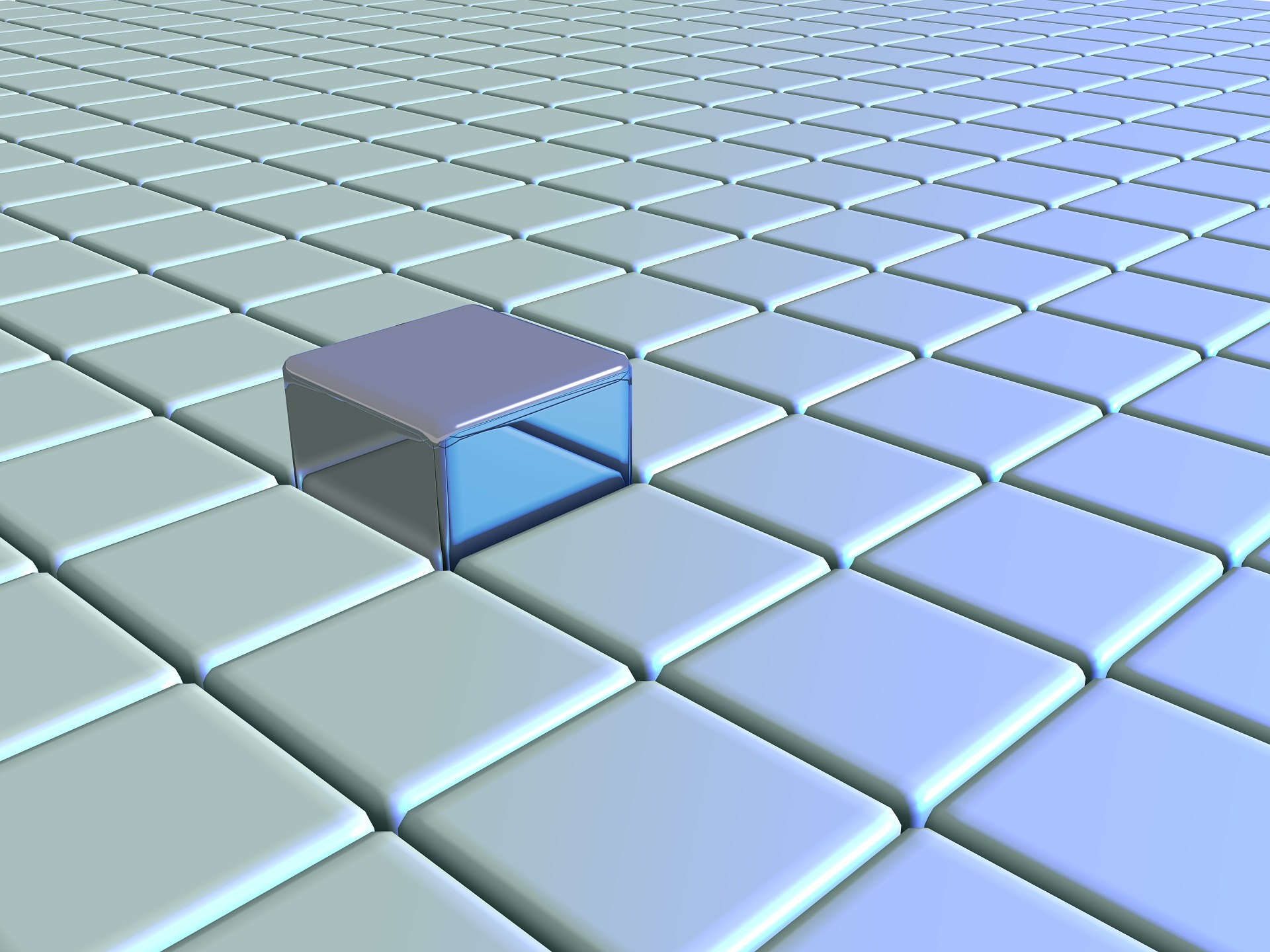
Each cell within planar NAND flash memory stores charge in a way similar to how a bucket stores water. By considering an imaginary line half-way up the bucket we can assign a binary one or zero based on whether the bucket contains more or less water than the line. Thus a full bucket, or a fully-charged NAND cell, denotes a zero while an empty bucket / cell denotes a one… assuming we are considering SLC, where each bucket stores one bit.
Moving to MLC (two bits) or TLC (three bits) is therefore a case of adding more lines, allowing us to differentiate between more states within the same bucket. The benefit is double (MLC) or quadruple (TLC) density but the drawback is that there will be a lower margin for error when measuring the amount of water/charge stored. As a consequence, the actions of reading, writing and erasing take longer while the endurance of the cell also drops drastically (leaky buckets are more of a problem as you try to be more precise about the measurements). The original article covers this all in more detail.
Shrinking Lithographies
If you remember, I also talked about the way that flash memory manufacturers are constantly shrinking the size of NAND flash cells in order to make increasingly dense packages, thus reducing the cost – but that the technology was now approaching its physical limits. In the bucket example, just imagine that the buckets are getting smaller and smaller. This is initially a good thing because smaller buckets (actually floating gate transistors) mean more buckets can fit in the same overall space, but in time the buckets become so small that they are no longer manageable – and then the technology hits a brick wall.
So Why Is It 2D?
In NAND flash memory, sets of cells are connected together in a string to form a NAND gate:

If you consider one of the pieces of silicon substrate contained inside a flash chip as a rectangle with dimensions X and Y, each one of these strings of cells will take up some space stretching out in one of these two dimensions. Shrinking the lithography, i.e. manufacturing everything on a smaller scale, will give us the opportunity to fit more strings on the same about of substrate. But as we previously discussed, there comes a point when things are simply too small and too close together, resulting in interference and leakage.
3D NAND: Going Vertical

The cost of a semiconductor is proportional to the die size. It is therefore a good thing for the cost if more electronics can be crammed into the same tiny piece of silicon. The fundamental difference in 3D NAND, which gives rise to its name, is that the strings previously described are now arranged vertically – another words in the Z dimension. For this reason, Samsung calls the technology V-NAND.
Imagine the string of cells shown earlier, but this time stood on its end and then folded in two to make a U shape. We now have a vertical string which takes up only a fraction of the original space in the X and Y dimensions. What’s more, we can continue to build in the Z dimension as manufacturing processes allow. Samsung’s first generation of V-NAND had strings of 24 layers, while the second generation had 32. The latest 3rd generation now has 48. And as Jim Handy explains, there are few theoretical limits on the number of layers possible. (Just to be clear, these layers are all within the same “wafer” of silicon, otherwise there would be no cost benefit…)
Crucially, since the move to a Z dimension relieves the pressure on the X and Y dimensions, 3D flash is actually free to return to a slightly larger lithography, thus avoiding all of the nasty problems that 2D planar NAND was starting to hit as it approached the 10nm range.
Charge Trap Flash and 3D TLC
Aside from the vertical stacking, there is another fundamental change with 3D NAND – it no longer uses floating gate transistors (yes, that’s right, the buckets from earlier). Instead, it uses a technology called Charge Trap Flash. I’m not going to attempt an explanation of CTF here, but it was memorably described by Samsung as like using cheese instead of water. So, instead of the buckets from earlier, picture cheese.
This cheese has a number of benefits over floating gate transistors in terms of endurance and power consumption, but it still works in a similar way in terms of the number of bits that can be stored – in other words SLC, MLC and TLC. However, because of its better endurance rates, with 3D NAND it is now a realistic proposition to use TLC to replace 2D planar MLC (something my employer Kaminario has already embraced).
This is big news. The cost per density of 3D TLC NAND flash is revolutionary, with plenty of room for further developments as the flash fabricators add more layers. Three years ago it looked like NAND flash was a technology in terminal decline, but with 3D techniques the future is bright. We might even get to a point soon where we see the introduction of…
Quad-Level Cell (QLC) Flash
If the endurance of CTF-based 3D NAND is acceptable, it’s not hard to envisage one of the flash fabricators releasing a quadruple-level cell version of the medium. The potential benefit is an order-of-magnitude increase in density for roughly the same cost.
After all, everybody wants more cheese… right?
This article is part of the Storage for DBAs series. If you found this series useful, you might also be interested in Databases in the Age of AI, which explores how AI agents are changing the assumptions at the heart of enterprise data systems.

Any followup since this article?
It was very informative.
I would like to know more about the research on how long bits stay in a cell.
I have 20 years old data, moved from floppy to harddrive, to harddrive, to CD to DVD, to harddrive, and now I want to move it to SSD. I want to know more about data retention.
I recommend starting with this article on AnandTech:
http://www.anandtech.com/show/9248/the-truth-about-ssd-data-retention
Thank you for writing this highly informative piece.
It would be useful to know exactly how much bit density improvement we obtain in practice from going from 2D planar to 3D. Going backward to older process nodes reduces bit density. Adding vertical traces (?) consumes die real estate.
So, all in all how much does bit density improve by on an 8 mm x 8 mm die?
I’m really not sure that information like that concerning bit density is easily obtainable, especially for 3D NAND. The flash fabricators are all working on their own methods to outdo each other and so bit density is improving all the time, but not necessarily in a linear fashion. Truth be told, I just don’t know.
But if you are interested in learning about the subject in more detail, I can highly recommend you reading the blog articles from Jim Handy of Objective Analysis:
http://thememoryguy.com/
3D nand, is basically 2 or 3 layers of 2D nand layered on top of one another. It’s not a true 3D (meaning going from square to cube system).
Currently it appears to be pretty linear with the amount of layers (tri-level cells are 1/3rd larger in capacity than dual layers for about the same square surface area, and MLC is 1/2 more than SLC.
The increase in size is mainly in the height of a chip; which matters less, as the height of the actual silicon is a few micrometers high; resulting in 3 to 4x more density, for the same chip size.
Which is why you can now see 256GB and 512GB MicroSD cards.
They could theoretically put 8 layers on top of one another, resulting in almost 1TB on a microSD Card, but with those chips, heat becomes an issue, and thus the chip needs to have a built in cooling system. Maybe our future card readers will be equipped with aluminum or copper cooling plates, cooled by a fan or device chassis.
Unless I am misunderstanding your point, I do not agree with you. 3D NAND is the “vertical” arrangement of strings of NAND gates (originally floating gate transistors, but in 3D they are typically charge traps). The word “vertical” is used in the context of the Z dimension, whereby the X and Y dimensions are those used by 2D or “planar” NAND and Z is perpendicular to this plane.
The first commercially available 3D NAND was Samsung’s 24 layer V-NAND, which was superseded by 32 layers and then 48 layers. We now see the likes of SK Hynix and Western Digital announcing 72 and 96 layer products, with 128 layers on the horizon.
Correction on above, the MLC/SLC should have read multi layered, single layered.
MLC and SLC technology is something totally different!