In recent articles in this series I’ve been looking at the architectural choices for building All Flash Arrays (AFAs). I surmised that there are three main approaches:
- Hybrid Flash Arrays
- SSD-based All Flash Arrays
- Ground-Up All Flash Arrays (which from here on I’ll refer to as Custom Flash Module arrays or CFM arrays)
I’ve already blown metaphorical raspberries at the hybrid approach, so now it’s time to cover the other two.
SSD or CFM: The Big Question
I think the most interesting question in the AFA industry right now is the one of whether the SSD or CFM design will win. Of course, it’s easy to say “win” like that as if it’s a simple race, but this is I.T. – there’s never a simple answer. However, the reality is that each method offers benefits and drawbacks, so I’m going to use this blog post to simply describe them as I see them.
Before I do that, let me just remind you of what the vendor landscape looks like at this time:
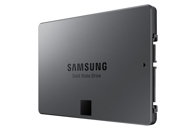
SSD-based architecture: Right now you can buy SSD-based arrays from EMC (XtremIO), Pure Storage, Kaminario, Solidfire, HP 3PAR and Huawei to name a few. It’s fair to say that the SSD-based design has been the most common in the AFA space so far.
CFM-based architecture: On the other hand, you can now buy ground-up CFM-based arrays from Violin Memory, IBM (FlashSystem), HDS (VSP), Pure Storage (FlashArray//m) and EMC (DSSD). The latter has caused some excitement because of DSSD’s current air of mystery in the marketplace – in other words, the product isn’t yet generally available.
So which approach is “the best”?
The SSD-based Approach
If you were going to start an All Flash Array company and needed to bring a product to market as soon as possible, it’s quite likely you would go down the SSD route. Apart from anything else, flash management is hard work – and needs constant attention as new types of flash come to market. A flash hardware engineer friend of mine used to say that each new flash chip is like a snowflake – they all behave slightly differently. So by buying flash in the ready-made form of an SSD you bypass the requirement to put in all this work. The flash controller from the SSD vendor does it for you, leaving you to concentrate on the other stuff that’s needed in enterprise storage: resilience, availability, data services, etc.
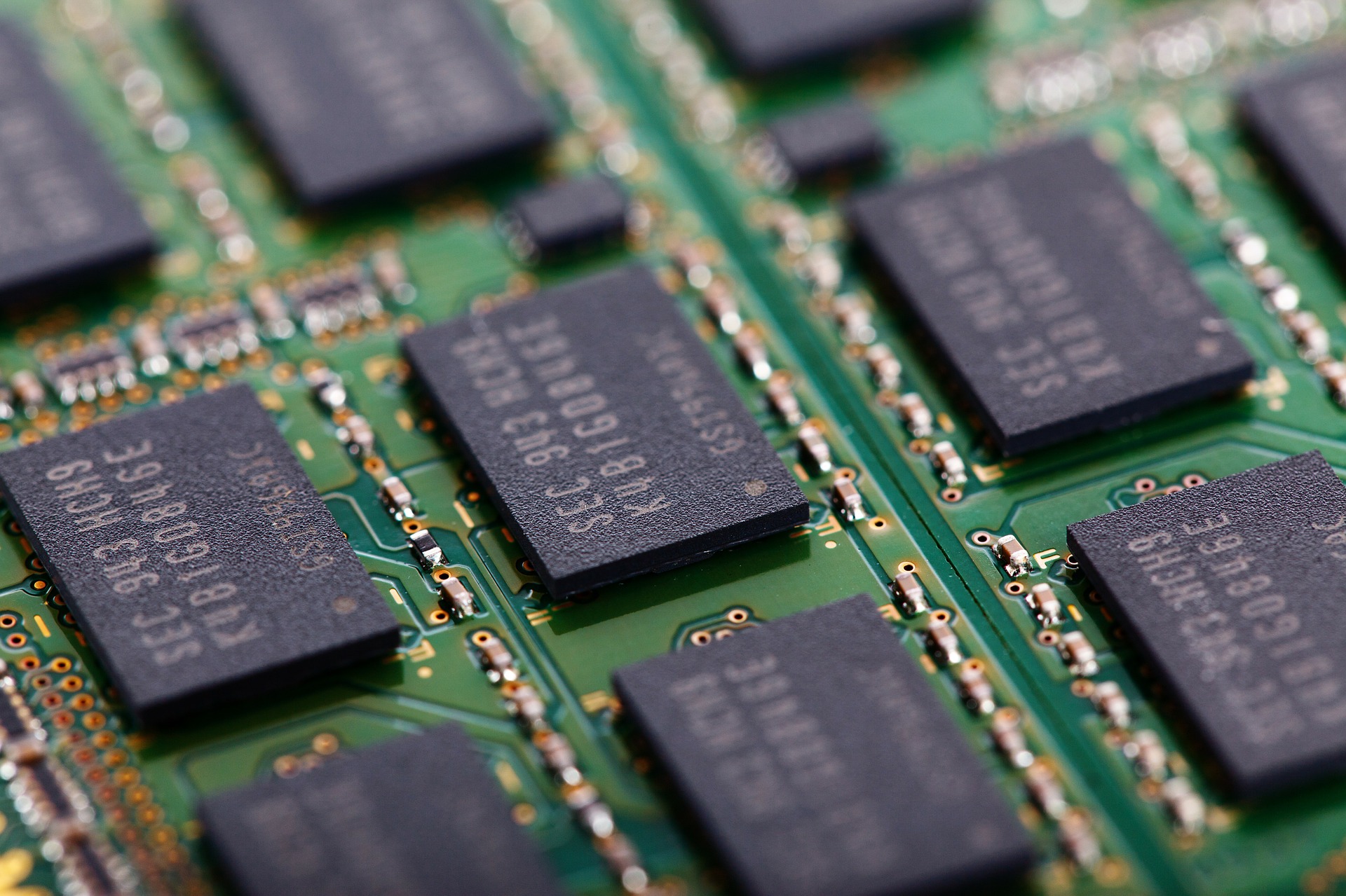
On the other hand, it seems clear that an SSD is a package of flash pretending to behave like a disk. That often means I/Os are taking place via protocols that were designed for disk, such as Serial Attached SCSI. Also, in a unit the size of an all flash array there are likely to be many SSDs… but because each one is an isolated package of flash, they cannot work together and manage the flash holistically. In other words, if one SSD is experiencing issues due to garbage collection (for example), the others cannot take the strain.
The Ground-Up Approach
For a number of years I worked for Violin Memory, which adopted the ground-up approach at its very core. Violin’s position was that only the CFM approach could unlock the full potential benefits from NAND flash. By tightly integrating the NAND flash into its array – and by using its own controllers to manage that flash – Violin believed it could deliver the best performance in the AFA market. On the other hand, many SSD vendors build products for the consumer market where the highest levels of performance simply aren’t necessary. All that’s required is something faster than disk – it doesn’t always have to be the fastest possible solution.
It could also be argued that any CFM vendor who has a good relationship with a flash fabricator (for example, Violin was partly-owned by Toshiba) could gain a competitive advantage by working on the very latest NAND flash technologies before they are available in SSD form. What’s more, SSDs represent an additional step in the process of taking NAND flash from chip to All Flash Array, which potentially means there’s an extra party needing to make their margin. Could it be that the CFM approach is more cost effective? [Update from Jan 2017: Violin Memory has now filed for chapter 11 bankruptcy protection]
SSD Economics
The argument about economics is an interesting one. Many technical people have a tendency to focus on what they know and love: technology. I’m as guilty of this as anyone – given two solutions to a problem I tend to gravitate toward the one that has the most elegant technical design, even if it isn’t necessarily the most commercially-favourable. Taking raw flash and integrating it into a custom flash module sounds great, but what is the cost of manufacturing those CFMs?

Manufacturing is all about economies of scale. If you design something and then build thousands of them, it will obviously cost you more per unit than if you build millions of them. How many ground-up all flash vendors are building their custom flash modules by the millions? In May 2015, IBM issued this press release in which they claimed that they were the “number one all-flash storage array vendor in 2014“. How many units did they ship? 2,100.
In just the second quarter of 2015, almost 24 million SSDs were shipped to customers, with Samsung responsible for 43.8% of that total (according to US analyst firm Trendfocus, Inc). Who do you think was able to achieve the best economy of scale?
Design Agility
The other important question is the one about New Stuff ™. We are always being told about fantastic new storage technologies that are going to change our lives, so who is best placed to adopt them first?
Again there’s an argument to be made on both sides. If the CFM flash vendor is working hand-in-glove with a fabricator, they may have access to the latest technology coming down the line. That means they can be prepared ahead of the pack – a clear competitive advantage, right?
But how agile is the CFM design? Changing the NVM media requires designing an entirely-new flash module, with all the associated hardware engineering costs such as prototyping, testing, QA and limited initial manufacturing runs.
For an SSD all flash array vendor, however, that work is performed by the SSD vendor… again somebody like Samsung, Intel or Micron who have vast infrastructures in place to perform that sort of work all the time. After all, a finished SSD must behave exactly like a disk, regardless of what NVM technology it uses under the covers.
Conclusion

There are obviously two sides to this argument. The SSD was designed to replace a fundamental bottleneck in storage systems: the hard disk drive. Ironically, it may be the fate of the SSD to become exactly what it replaced. For flash to become mainstream it was necessary to create a “flash-behaving-as-disk” package, but the flip side of this is the way that SSDs stifle the true potential of the underlying flash. (Although perhaps NVMe technologies will offer us some salvation…)
However, unless you are a company the size of Samsung, Intel or Micron it seems unlikely that you would be able to retain the manufacturing agility and economies of scale required to produce custom flash modules at the price point of SSDs. Nor would you be likely to have the agility to adopt new NVM technologies at the moment that they become economically preferable to whatever medium you were using previously.
Whatever happens, you can be sure that each side will claim victory. With the entire primary data market to play for, this is a high stakes game. Every vendor has to invest a large amount of money to enter the field, so nobody wants to end up being consigned to the history books as the Betamax of flash…
For younger readers, Betamax was the loser in a battle with VHS over who would dominate the video tape market. You can read about it here. What do you mean, “What is a video tape?” Those things your parents used to watch movies on before the days of DVDs. What do you mean, “What is a DVD?” Jeez, I feel old.
This article is part of the Storage for DBAs series. If you found this series useful, you might also be interested in Databases in the Age of AI, which explores how AI agents are changing the assumptions at the heart of enterprise data systems.

Hi, I believe that NVM can help, but the big issue is about the PCI lanes that processor and motherboard can support.
If you look in the Oracle Exadata X5 EF with NVMe Intel Drivers (http://www.oracle.com/technetwork/database/exadata/exadata-x5-2-ds-2406241.pdf) you have two E5-2630 v3 with 40 PCI lanes each one, but QDR Infiniband (PCI x16), + 4 PCI 8x Oracle PCIe NVMe Switch Card’s (http://docs.oracle.com/cd/E54943_01/html/E54944/gouab.html#scrolltoc), + 10G network. So, make the count, a full system will not work and suffer bottleneck.
You need to start limit the number of drivers in every switch card (only two), and because every driver receive 4 PCI Lanes (http://www.oracle.com/technetwork/server-storage/sun-x86/documentation/x5-2l-system-architecture-2328119.pdf) your PCI 8x is full with only two drivers.
NVM can help, but need to change more than just drivers.
I understand what you are saying but I believe you are talking about NVMe in servers rather than storage arrays. I am talking about the design of all-flash storage area networks…
Yes, I know and understand it. But for Oracle databases, Exadata is one big player and this points can be important. By the way, NVM is parallelism and a lot of drivers doing a lot of things in parallel need a good system (Exadata or no).
Speaking of NVMe, you might want to take a look at the FlashGrid software approach using NVMe SSDs in standard x86 servers. It’s a converged compute+storage architecture designed specifically for Oracle RAC/ASM. Also check this white paper for bandwidth numbers compared to XtremIO: https://www.flashgrid.io/wp-content/uploads/2015/10/FlashGrid_Intel_P3700_SSD_wp.pdf
Cheeky