Skip to content
Unknown's avatar

flashdba

Database Systems Under Pressure

  • Storage for DBAs
  • Databases in the Cloud
  • Databases in the Age of AI
  • About

Category: Storage for DBAs

All Flash Arrays: Where’s My Capacity? Effective, Usable and Raw Explained

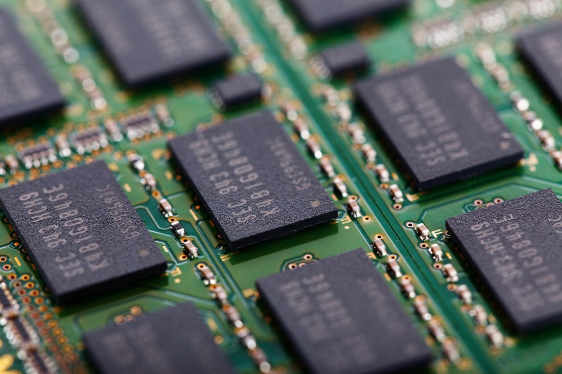
All flash array vendors quote capacity in three very different ways – raw, usable and effective. This article explains the differences, warns against vendor smoke and mirrors, and argues that usable capacity at 1:1 reduction is the only figure that matters when buying.

flashdba All Flash Arrays, Blog, Storage, Storage for DBAs 2 Comments October 6, 2015June 5, 2026 7 Minutes

All Flash Arrays: Can’t I Just Stick Some SSDs In My Disk Array?

Filling a legacy disk array with SSDs doesn't make it a true all flash array. This article builds a disk array from first principles to show why every architectural decision made for disk turns out to be the wrong one for flash.

flashdba All Flash Arrays, Blog, Storage, Storage for DBAs 6 Comments August 18, 2015June 4, 2026 7 Minutes

All Flash Arrays: What Is An AFA?

All Flash Arrays - Hybrid, SSD-based or Ground-Up

All flash arrays come in three distinct categories: hybrid, SSD-based and ground-up designs. This article explains the differences, cuts through competing industry definitions from IDC and Gartner, and sets out a clear definition for what actually qualifies as an AFA.

flashdba All Flash Arrays, Blog, Storage, Storage for DBAs Leave a comment June 25, 2015June 6, 2026 5 Minutes

Understanding Flash: Summary – NAND Flash Is A Royal Pain In The …

NAND flash is a genuinely difficult storage medium – it wears out, has slow erases, and requires complex management. This article summarises the Understanding Flash series and explains why architecture is what separates great all-flash arrays from merely fast ones.

flashdba Blog, Storage, Storage for DBAs, Understanding Flash 2 Comments May 14, 2015June 4, 2026 5 Minutes

Understanding Flash: Fabrication, Shrinkage and the Next Big Thing

NAND flash manufacturers have been shrinking transistors for decades, but 2D planar NAND is hitting its physical limits. This article explains process geometries, 3D NAND as the answer, and why new memory technologies face a billion-dollar barrier to market.

flashdba Blog, Storage, Storage for DBAs, Understanding Flash 3 Comments February 17, 2015June 4, 2026 6 Minutes

Understanding Flash: Floating Gates and Wear

NAND flash wears out because repeated program and erase operations degrade the oxide layer in floating gate transistors. This article explains how flash cells store data and why wear affects SLC, MLC and TLC differently.

flashdba Blog, Storage, Storage for DBAs, Understanding Flash 9 Comments January 9, 2015June 4, 2026 10 Minutes

Understanding Flash: Unpredictable Write Performance

Not all NAND flash writes are equal. MLC flash has fast pages and slow pages, creating unpredictable write latency unless the storage controller manages them intelligently. This article explains why write performance varies and what enterprise arrays do about it.

flashdba Blog, Storage, Storage for DBAs, Understanding Flash 6 Comments December 10, 2014June 4, 2026 5 Minutes

Understanding Flash: The Write Cliff

When flash garbage collection cannot keep pace with incoming writes, performance falls off a cliff. This article explains background versus active garbage collection, write amplification and why predictability matters more than peak speed.

flashdba Blog, Storage, Storage for DBAs, Understanding Flash 4 Comments November 24, 2014June 3, 2026 6 Minutes

Understanding Flash: Garbage Collection Matters

NAND flash can only be erased at the block level, not the page level. Garbage collection is the process that recycles stale pages to keep a flash system writable – and without it, performance collapses. This article explains why.

flashdba Blog, Storage, Storage for DBAs, Understanding Flash 19 Comments October 15, 2014June 3, 2026 5 Minutes

Understanding Flash: The Flash Translation Layer

Electronic components on a circuit board, representing the hardware layer managed by the flash translation layer

The flash translation layer is the hidden software layer that makes NAND flash usable as enterprise storage. This article explains logical block mapping, wear levelling, garbage collection and write amplification.

flashdba Blog, Storage, Storage for DBAs, Understanding Flash 11 Comments September 17, 2014June 3, 2026 6 Minutes

Posts navigation

Older posts
Newer posts
Blog at WordPress.com.
flashdba
Blog at WordPress.com.
  • Subscribe Subscribed
    • flashdba
    • Join 444 other subscribers
    • Already have a WordPress.com account? Log in now.
    • flashdba
    • Subscribe Subscribed
    • Sign up
    • Log in
    • Report this content
    • View site in Reader
    • Manage subscriptions
    • Collapse this bar

Loading Comments...