In a proud moment for me, it appears that Mark Hurd, CEO of Oracle, has mentioned my flashdba blog during the Oracle Q4 2015 results call. At least, that’s what I’m reading into this section from the transcript published by Seeking Alpha:
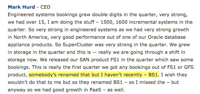
We grew in storage in the quarter and this is — really we are going through a shift in storage now. We released our SAN product FS1 in the quarter which saw some bookings. This is really the first quarter we got any bookings out of FS1 or GFS product, somebody’s renamed that but I haven’t recently – BS1. I wish they wouldn’t do that to me but so they renamed BS1 – so I missed the – but anyway so we had good growth in PaaS – as well.
I’m pretty sure that my blog post entitled Postcard from Oracle OpenWorld 2014: The Oracle FS1 Flash Array was the first place in which Oracle’s newly-announced FS1 Flash Storage System was ironically described as the “BS1 Flash Storage Array” due to some of the baffling marketing claims made at its announcement during Oracle OpenWorld 2014. Claims like, “The Oracle FS1 is the first mainstream, general purpose flash array”.
I haven’t heard the recording of the call, just read the transcript, but it appears to me that Mr Hurd uses the BS1 phrase to get some laughs from the analysts on the call.
So hey, thanks Mark! It’s exciting to know that finally, even in a small way, I’ve been able to make a contribution at the highest levels within Oracle. I am open to discussions about filling a new role as Oracle’s SVP of Investor Comedy Moments. And with those results, it could be an increasingly essential role…!
So this is it – the last article in my mini-series on understanding flash. This is the bit where I draw it all together in a neat conclusion that makes you think, “Yes! That was worth reading”. No pressure eh?
So let me start with the conclusion first: as a storage medium, NAND flash is a royal pain in the ass.
Chaos
Why? Well, let’s look back at what we’ve learned in the previous 9 articles:
Complex mapping tables are required to write updated data to free pages and track stale pages prior to erasure
The process of garbage collection (the recycling of stale pages) requires the over-provisioning of flash
The phenomenon of write amplification causes many more writes to take place on the backend than those issued from any hosts, negatively affecting performance and endurance
The fabrication plants (or “flash foundries”) built to manufacture NAND flash are incredibly expensive
In short, NAND flash is a tricky medium to use for enterprise storage. A whole lot of work is required to make a collection of flash chips appear to be a unified, resilient block of storage with fast, predictable performance.
And I haven’t even told you everything. Consider, for example, the phenomenon of read disturb. When you read a page within a NAND flash chip, you cause a very minor electronic field in the locality of the cells it contains. That field will cause a small disturbance to any neighbouring cells – usually not enough to cause concern, but significant nevertheless. So what happens when you repeatedly read that page? Eventually, after X number of reads, the data stored within the nearby cells becomes questionable.
The solution, therefore, is to keep track of the number of times each page is disturbed in this manner and then set a threshold (let’s say 50 disturbances) beyond which you will copy the data out to a clean page and then mark the old page as stale. Easy.
But just think about what that means for a moment. Remember when I said that write amplification was mainly impacted by write workloads? This new piece of information means that even on a 100% read workload there will be additional back-end writes taking place on the array. Just another example of why flash is a tricky medium to manage.
Order
Of course, it would be remiss of me not to mention that NAND flash brings a tremendous set of benefits along with these problems. You could say they come as a package (oh come on, that was one of my better puns).
Let’s go back to basics for a moment: if you want to take a defined quantity of work and do it in a shorter amount of time, what are your choices? Put simply, there are two options: do the same work faster, or do more of it in parallel (and of course both options can be used together for extra gain).
The basic building block of a disk array is, obviously, the hard disk drive. I’ve already explained at tedious length about the performance gap between disk and flash, so we know that we can access data faster using flash. Technologies like RAID allow multiple disks to be used in parallel to achieve performance (and resilience) gains, but given a limited amount of physical space (such as a data centre rack), how many hard drives can you actually squeeze into one system?
Now compare this to the number of NAND flash packages you could fit into the same space, all of which you could potentially utilise in parallel and at a lower latency. Doing the same work faster – and doing more of it in parallel.
Image courtesy of Google Inc.
And there’s more. Those clunky great big cabinets of disk use up horrendous amounts of power just to spin those little rotating platters – with much of the energy converted to heat and noise: waste. The heat results in a requirement for additional cooling, which uses even more power: more waste. And it all takes up so much physical space that data centres become overrun with storage.
In contrast, all flash arrays (AFAs) require less power, less cooling and take up less physical space: it’s not uncommon for customers to pay for the move to flash simply by avoiding the need to build a new data centre or extend an existing one. In summary, the net cost of using flash is now less than that of using disk.
When I first started writing this blog back in 2012 there was still a debate over whether flash would replace disk for enterprise storage. That debate was over some time ago: flash has already won.
Architecture Matters
So this post marks the end of my journey into explaining and understanding NAND flash. Yet there is a whole new area which needs exploring: the architecture of all flash arrays.
Enterprise storage needs be safe, reliable, predictable and fast. Yet at a package level, NAND flash is a tricky little beast that has to be constantly watched to make sure it behaves itself. There’s a dichotomy here: how do we use the latter to deliver the former? How do we take a component designed for consumer electronics and use it to build an enterprise-class AFA? In short, how we derive order from chaos?
The answer is in the architecture. At the time of writing this blog there are a number of AFA vendors on the market, each with a different approach to taming the beast. Apart from my own employer, Violin Memory, there is EMC, IBM, HDS, Pure Storage, SolidFire, Kaminario and a whole load more.
And that’s why this industry is so interesting to me. Everybody is trying to do this differently, although you can broadly categorise the solutions into three distinct ranges: hybrid arrays, SSD-based arrays and ground-up arrays. Everybody thinks their way is right – and nobody can afford to be wrong. The market for flash-based primary storage is huge and growing all the time: the winners get unparalleled success, while the losers … are simply left in disarray*
*I won’t lie – I’m so proud of that pun I’m going to award myself a couple of weeks off.
Storage architecture shapes database behaviour – and that relationship is evolving again. If you found this series useful, you might also be interested in Databases in the Age of AI, which explores how AI agents are changing the assumptions at the heart of enterprise data systems.
This is a very simple post to show the results of some recent testing that Tom and I ran using Oracle SLOB on Violin to determine the impact of using virtualization. But before we get to that, I am duty bound to write a paragraph of text featuring lots of long sentences peppered with industry buzz words. Forgive me, it’s just the way I’m wired.
It is increasingly common these days to find database environments running in virtual machines – even large, business critical ones. The driver is the trend to commoditize I.T. services and build consolidated, private-cloud style solutions in order to control operational expense and increase agility (not to mention reduce exposure to Oracle licenses). But, as I’ve said in previous posts, the catalyst has been the unblocking of I/O as legacy disk systems are replaced by flash memory. In the past, virtual environments caused a kind of I/O blender effect whereby I/O calls become increasingly randomized – and this sucked for the performance of disk drives. Flash memory arrays on the other hand can deliver random I/O all day long because… well, if you don’t know the reasons by now can I just recommend starting at the beginning. The outcome is that many large and medium-sized organisations are now building database-as-a-service platforms with Oracle databases (other database products are available) running in virtual machines. It’s happening right now.
Phew. Anyway, that last paragraph was just a wordy way of telling you that I’m often seeing Oracle running in virtual machines on top of hypervisors. But how much of a performance impact do those hypervisors have? Step this way to find out.
The Contenders
When it comes to running Oracle on a hypervisor using Intel x86 hardware (for that is what I have available), I only know of three real contenders:
Hyper-V has been an option for a couple of years now, but I’ll be honest – I have neither the time nor the inclination to test it today. It’s not that I don’t rate it as a product, it’s just that I’ve never used it before and don’t have enough time to learn something new right now. Maybe someday I’ll come back and add it to the mix.
In the meantime, it’s the big showdown: VMware versus Oracle VM. Not that Oracle VM is really in the same league as VMware in terms of market share… but you know, I’m trying to make this sound exciting.
The Test
This is going to be an Oracle SLOB sustained throughput test. In other words, I’m going to build an Oracle database and then shovel a massive amount of I/O through it (you can read all about SLOB here and here). SLOB will be configured to run with 25% of statements being UPDATEs (the remainder are SELECTs) and will run for 8 hours straight. What we want to see is a) which hypervisor configuration allows the greatest I/O bandwidth, and b) which hypervisor configuration exhibits the most predictable performance.
This is the configuration. First the hardware:
Violin Memory 6616 flash Memory Array
1x Dell PowerEdge R720 server
2x Intel Xeon CPU E5-2690 v2 10-core @ 3.00GHz [so that’s 2 sockets, 20 cores, 40 threads for this server]
128GB DRAM
1x Violin Memory 6616 (SLC) flash memory array [the one that did this]
8GB fibre-channel
And the software:
Hypervisor: VMware ESXi 5.5.1
Hypervisor: Oracle VM for x86 3.3.1
VM: Oracle Linux 6 Update 5 (with the Unbreakable Enterprise v3 Kernel 3.6.18)
Each VM is configured with 20 vCPUs and is using Linux Device Mapper Multipath and Oracle ASMLib. ASM is configured to use one single +DATA disgroup comprising 8 ASM disks (LUNs from Violin) with external redundancy. The database parameters and SLOB settings are all listed on the SLOB sustained throughput test page.
Results: Bare Metal (Baseline)
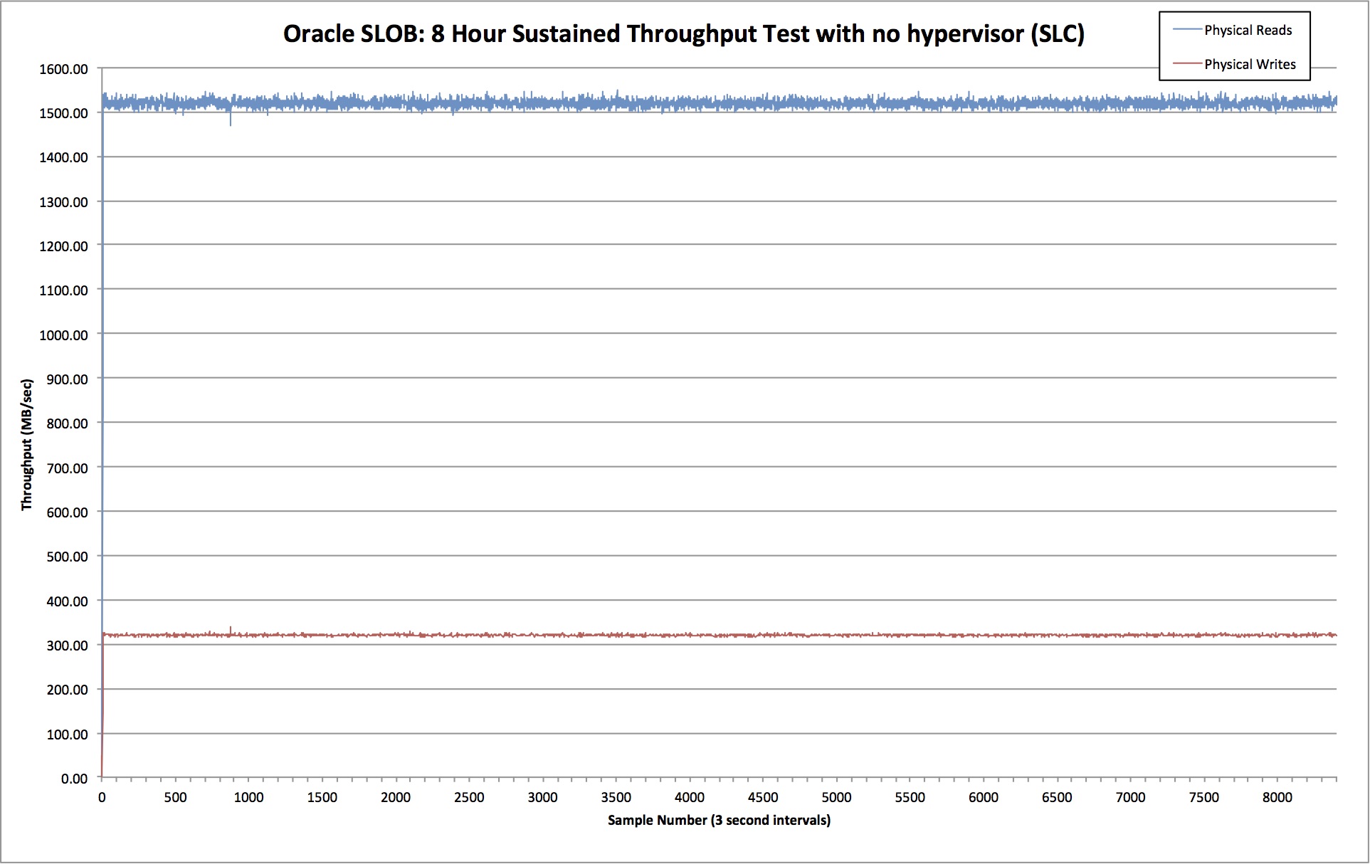
First let’s see what happens when we don’t use a hypervisor at all and just run OL6.5 on bare metal:
Ok so we’re looking at 1519 MB/sec of read throughput and 320 MB/sec of write throughput. Crucially, the lines are nice and consistent – with very little deviation from the mean. By dividing the amount of time spent waiting on db file sequential read(i.e. random physical reads) with the number of waits, we can calculate that the average latency for random reads was 438 microseconds.
Now we know what to expect, let’s look at the result from the hypervisor tests.
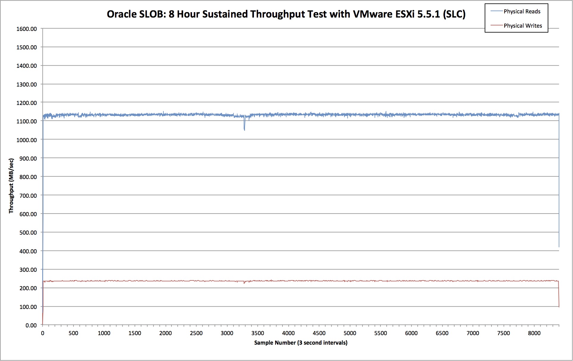
Results: VMware vSphere
VMware is configured to use Raw Device Mapping (RDM) which essentially gives the benefits of raw devices… read here for more details on that. Here are the test results:
Average read throughput for this test was 1133 MB/sec and write throughput averaged at 237 MB/sec. Average read latency was 596 microseconds. That’s an increase of 36%.
In comparison to the bare metal test, we see that total bandwidth dropped by around 25%. That might seem like a lot but remember, we are absolutely hammering this system. A real database is unlikely to ever create this level of sustained I/O. In my role at Violin I’ve been privileged to work on some of the busiest databases in Europe – nothing is ever this crazy (although a few do come close).
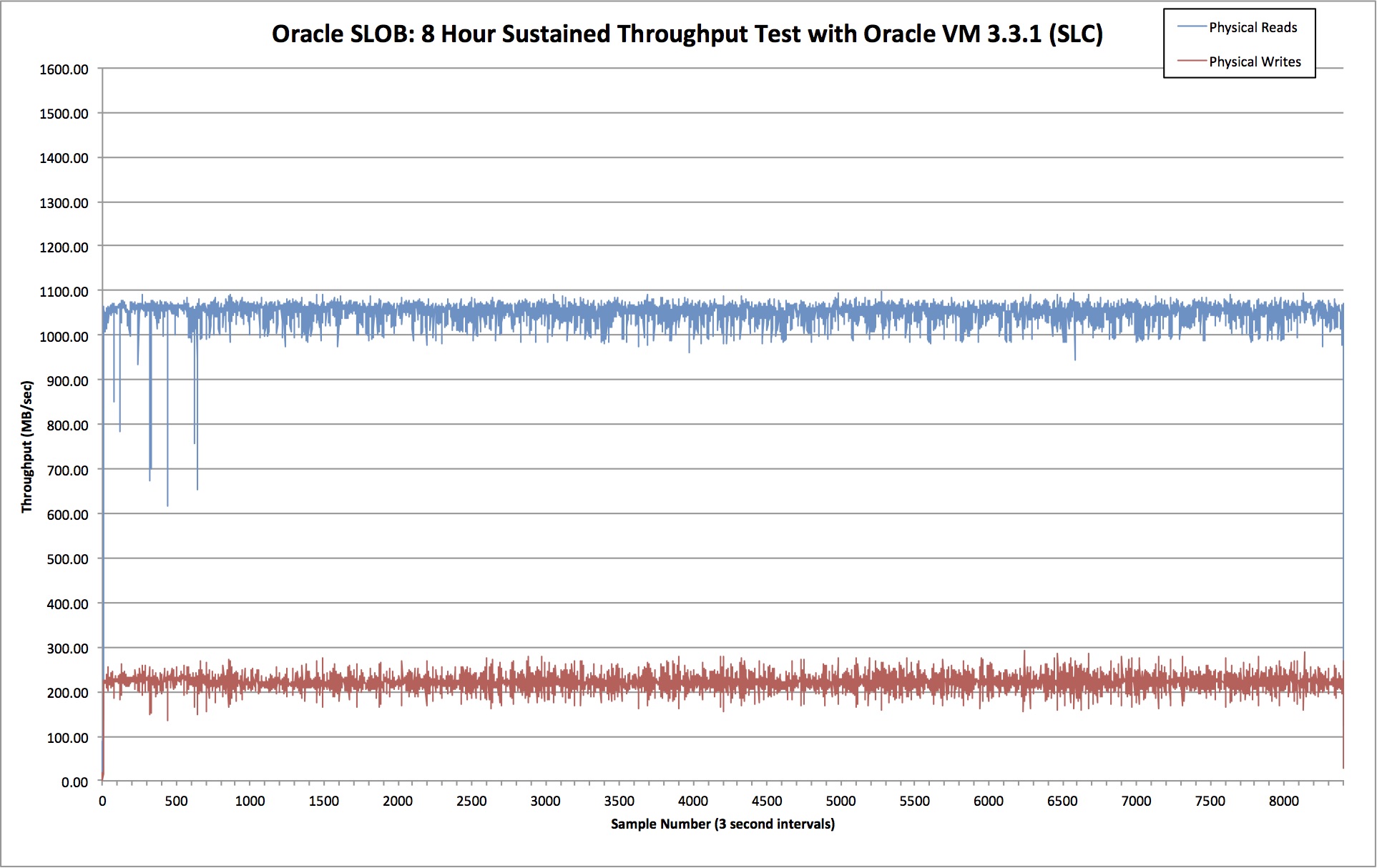
Results: Oracle VM
Oracle VM is based on the Xen hypervisor and therefore uses Xen virtual disks to present block devices. For this test I downloaded the Oracle Linux 6 Update 5 template from Oracle’s eDelivery site. You can see more about the way this VM was configured here. Here are the test results:
This time we see average read bandwidth of 1052MB/sec and average write bandwidth of 222MB/sec, with the average read latency at 607 microseconds, which is 39% higher than the baseline test.
Meanwhile, total bandwidth dropped by 31%. That’s slightly worse than VMware, but what’s really interesting is the deviation. Look at how ragged the lines are on the OVM test! There is a much higher degree of variance exhibited here than on the VMware test.
Conclusion
This is only one test so I’m not claiming it’s conclusive. VMware does appear to deliver slightly better performance than OVM in my tests, but it’s not a huge difference. However, I am very much concerned by the variance of the OVM test in comparison to VMware. Look, for example, at the wait event histograms for db file sequential read:
Wait Event Histogram
-> Units for Total Waits column: K is 1000, M is 1000000, G is 1000000000
-> % of Waits: value of .0 indicates value was <.05%; value of null is truly 0
-> % of Waits: column heading of <=1s is truly <1024ms, >1s is truly >=1024ms
-> Ordered by Event (idle events last)

                                                             % of Waits
                                          -----------------------------------------------
                                    Total
Hypervisor  Event                   Waits  <1ms  <2ms  <4ms  <8ms <16ms <32ms  <=1s   >1s
----------- ----------------------- ----- ----- ----- ----- ----- ----- ----- ----- -----
Bare Metal: db file sequential read 5557.  98.7   1.3    .0    .0    .0    .0
VMware ESX: db file sequential read 4164.  92.2   6.7   1.1    .0    .0    .0
Oracle VM : db file sequential read 3834.  95.6   4.1    .1    .1    .0    .0    .0    .0
The OVM tests show occasional results in the two highest buckets, meaning once or twice there were waits in excess of 1 second! However, to be fair, OVM also had more millisecond waits than VMware.
Anyway, for now – and for this setup at least – I’m sticking with VMware. You should of course test your own workloads before choosing which hypervisor works for you…
Thanks as always to Kevin for bringing Oracle SLOB to the community.
I’ve run into a few customers recently who have had problems with their ASM rebalance operations running too slowly. Surprisingly, there were some simple concepts being overlooked – and once these were understood, the rebalance times were dramatically improved. For that reason, I’m documenting the solutions here… I hope that somebody, somewhere benefits…
1. Don’t Overbalance
Every time you run an ALTER DISKGROUP REBALANCE operation you initiate a large amount of I/O workload as Oracle ASM works to evenly stripe data across all available ASM disks (i.e. LUNs). The most common cause of rebalance operations running slowly that I see (and I’m constantly surprised how much I see this) is to overbalance, i.e. cause ASM to perform more I/O than is necessary.
It almost always goes like this. The customer wants to migrate some data from one set of ASM disks to another, so they first add the new disks:
alter diskgroup data
add disk  'ORCL:NEWDATA1','ORCL:NEWDATA2','ORCL:NEWDATA3','ORCL:NEWDATA4',
          'ORCL:NEWDATA5','ORCL:NEWDATA6','ORCL:NEWDATA7','ORCL:NEWDATA8'
rebalance power 11 wait;
Then they drop the old disks like this:
alter diskgroup data
drop disk 'DATA1','DATA2','DATA3','DATA4',
          'DATA5','DATA6','DATA7','DATA8'
rebalance power 11 wait;
Well guess what? That causes double the amount of I/O that is actually necessary to migrate, because Oracle evenly stripes across all disks and then has to rebalance a second time once the original disks are dropped.
This is how it should be done – in one single operation:
alter diskgroup data
add disk  'ORCL:NEWDATA1','ORCL:NEWDATA2','ORCL:NEWDATA3','ORCL:NEWDATA4',
          'ORCL:NEWDATA5','ORCL:NEWDATA6','ORCL:NEWDATA7','ORCL:NEWDATA8'
drop disk 'DATA1','DATA2','DATA3','DATA4',
          'DATA5','DATA6','DATA7','DATA8'
rebalance power 11 wait;
A customer of mine tried this earlier this week and reported back that their ASM rebalance time had reduced by a factor of five!
By the way, the WAIT command means the cursor doesn’t return until the command is finished. To have the command essentially run in the background you can simply change this to NOWAIT. Also, you could run the ADD and DROP commands separately if you used a POWER LIMIT of zero for the first command, as this would pause the rebalance and then the second command would kick it off.
2. Power Limit Goes Up To 1024
Simple one this, but easily forgotten. From the early days of ASM, the maximum power limit for rebalance operations was 11. See here if you don’t know why.
From 11.2.0.2, if the COMPATIBLE.ASM disk group attribute is set to 11.2.0.2 or higher the limit is now 1024. That means 11 really isn’t going to cut it anymore. If you are asking for full power, make sure you know what number that is.
3. Avoid The Compact Phase (for Flash Storage Systems)
An ASM rebalance operation comprises three phases, where the third one is the compact phase. This attempts to move data as close as possible to the outer tracks of the disks ASM is using.
Did you spot the issue there? Disks. This I/O-heavy phase is completely pointless on a flash system, where I/O is served evenly from any logical address within a LUN.
You can therefore avoid that potentially-massive I/O hit by disabling the compact phase, using the underscore parameter _DISABLE_REBALANCE_COMPACT=TRUE. Remember that you need to get Oracle Support’s permission before setting underscore parameters! Point your SR in the direction of the following My Oracle Support note:
What is ASM rebalance compact Phase and how it can be disabled (Doc ID 1902001.1)
Unfortunately it appears the parameter was deprecated in 12c, so from now on you have to set the ASM diskgroup attribute “_rebalance_compact” to FALSE (note the opposite value to that set at the instance level!), for example:
ALTER DISKGROUP SET ATTRIBUTE "_rebalance_compact”="FALSE";
If you want to know more about this topic (for example, what the first two rebalance phases are), or indeed anything about ASM in general, I highly recommend the legendary ASM blogger that is Bane Radulovic a.k.a. ASM Support Guy.
Conclusion
An ASM rebalance potentially creates a lot of I/O, which means you may need to wait for a long time before it finishes. For that reason, make sure you understand what you are doing and make every effort to perform only as much I/O as you actually need. Don’t forget you can use the EXPLAIN WORK command to gauge in advance how much work is required.
I’m delighted to say that this is another guest post from my good friend Nate Fuzi, who performs the same role as me for Violin but is based in the US instead of EMEA. Because he is American, Nate thinks that scones are called “biscuits”, that chips are called “fries” and that there is nothing – *nothing* – that cannot be improved with the simple addition of bacon. Clearly, something is fundamentally wrong with him – and yet he is like a brother to me. Like the strange, American step-brother I only see a few times a year and whom I cannot understand without the use of a translator. But he’s family all the same. So over to you Nate… and remember: Mom loved me more.
Remember when your parent answering your whiny “but whyyyyyyy???” with “Because I said so” was something you just had to accept? It meant there was no more explanation coming, and it was time for you to move on. Over the years, that answer broke down, and you grew confident you were owed more. And parents agreed: the more you demonstrated your ability to reason, the more reason you got to help you over the denial. It’s a sign of respect that we pay each other in adult life. And it can feel like disrespect if the reason offered feels weak or like it is intended to discourage further inquiry.
I was recently faced with solving what seemed a straightforward problem: take an existing Linux server running EMC’s multipathing software, PowerPath or “PP” as I will refer to it here, to access LUNs presented from that company’s SAN product, the VNX array, and attach and run Violin storage alongside the VNX. PP didn’t then support Violin arrays (still doesn’t at the time of this writing), so what was the client to do when they wanted to try out Violin’s AFA for their database environments? Just run PP and native Linux multipathing, called DM-MPIO, side by side, letting PP manage the VNX LUNs and DM-MPIO manage I/Os bound for Violin, right?
PowerPath versus DM-MPIO
Wrong. Won’t work, I read. PowerPath does something at the HBA layer, I read a seemingly helpful web poster explain, that will corrupt either the VNX data or the Violin data. Well… maybe it will work, suggested another poster, but EMC might not support customers running in such a configuration. Others suggested ominously that PP and DM-MPIO don’t work well together… leaving it to the reader’s imagination what might result. I’m no master Googler, but I couldn’t find where anyone had put aside the rumors and vaguely threatening suggestions and actually tried it. Well, I did it, and I want to write about it so others know it can be done and how to do it because, well, those explanations I read didn’t stand up to question and felt like they were meant to scare me into not trying it. Of course I had to try it! Now, let’s be clear about what I am and am not saying: I am saying I have done this and it works. It’s in production at a customer site, running for months without issue. I am not saying that I have spoken to your EMC support rep and that you’ve been green-lighted to do this in your production environment. I’m not an EMC customer, and I don’t have a buddy in EMC support. So let’s consider this for informational purposes only for the time being.
First off, as several folks rightly pointed out, DM-MPIO could easily manage LUNs from both SAN products. Drop PP, configure DM-MPIO, and done. Well, that just sounds too simple. But it’s true: DM-MPIO has come a long way over the last few years and offers a pretty good set of features for free. PP costs money but is not without added value, as it does have additional configurability for reserve paths that become active in the event of a failure scenario, as well as IO distribution models beyond those offered by DM-MPIO, for example. My customer wanted to keep running PP, so this option was off the table for me.
Next up is the fun fact that PP advises you upon installation that you should “Blacklist all devices in /etc/multipath.conf and stop multipathd service”. The installer doesn’t say what will happen if you don’t do this, only that it is “*** IMPORTANT ***”. Check. Easy enough to ignore if this is the first thing you do. But if DM-MPIO is already running on the system and you try to start PP, it tells you this (verified in 5.7 and 6.0 only):
[root@host] # /etc/init.d/PowerPath start
Starting PowerPath:                                                      [FAILED]
Aborting PowerPath start since DM-Multipath is active.
Refer to PowerPath for Linux Installation and Administration Guide for more information
That’s a bummer. You actually have to stop multipathd and flush its paths before PP will start up. OK, I can do that. And, to be sure, you do NOT want both products attempting to manage IOs for the same device at the same time. That really is a bad thing. As we’ll see shortly, we might even want to segregate traffic across different FC ports, although this is strictly for optimization, not because you can’t mix traffic. But, as soon as we’ve installed the device-mapper-multipath-* packages, let’s honor this restriction right away by blacklisting the EMC devices in /etc/multipath.conf like this:
blacklist {
       devnode "^(control|vg|ram|raw|loop|fd|md|dm-|sr|scd|st)[0-9]*"    # standard stuff
       devnode "^hd[a-z][0-9]*"                                          # this line too
       device {
              vendor "DGC"
              product "*"
       }
       device {
              vendor "EMC"
              product "*"
       }
}
Note that the VNX line grew up in the Clariion company later acquired by EMC and presents a vendor string of “DGC”. Don’t ask me why. [Because the Clariion was a product from Data General Corporation? — flashdba 🙂] It is my understanding that VMAX arrays do present “EMC” as their vendor string. Having done this, we want to explicitly except Violin devices from getting blacklisted:
This isn’t completely necessary, but it does make clear our intentions: don’t manage VNX/EMC devices but do manage Violin devices. Having both entries in the file means that adding some third storage product to the FC SAN won’t cause it to get picked up by DM-MPIO without us consciously making it so. Belt and suspenders, they used to say.
Verify your multipath configuration without actually running it. Do this by adding the “-d” flag to your multipath command:
[root@host] # multipath -v3 -d
The “-v3” flag gives us a verbose parsing of the configuration file so we can see each device and whether, what, and why DM-MPIO is going to do that with device. Make changes ad nauseum, and once you like what you see, run the command without “-d”, and create your multipath devices.
Cool. But remember when PP refused to start up earlier, saying DM-MPIO was found running? Guess what: PP’s inexplicable method of editing your /etc/rc.d/rc.sysinit script to insert its startup lines means it doesn’t attempt to start up until after DM-MPIO gets started on reboot. (Take a look for yourself; it’s there. It also makes you manually start PP if you apply a kernel update that resets the contents of rc.sysinit, at which point it reinserts the startup lines. Sweet.) How to get around this? I’m sure there are lots of solutions. I created a script to flush existing multipaths and start up PP in /etc/init.d and linked it as /etc/rc.d/rc3.d/S86PowerPath. This makes it so PP gets called just prior to DM-MPIO, and each is happy. The later call in /etc/rc.d/rc.sysinit is then redundant but causes no harm. I suppose you could almost as easily edit the rc.sysinit script to remove the check–just remember to make the same edit if/when you update PP.
Now, what was that I said a bit ago about segregating traffic on different HBA ports? This is not required; no magic is happening on the HBA with either product. Each one will discover the devices it is concerned with via its own callout routine and handle that device how you configure it to. But let’s imagine you have 4 FC ports on your host and choose to allow PP and DM-MPIO to each manage devices across all those ports. Neither will be aware what the other is doing in terms of trying to optimize IO distribution across all paths available, and you could well end up shooting yourself in the foot with sub-optimal end results. Segregating traffic also allows you to set different HBA queue depths or optimization settings as recommended by each storage vendor, and we all want to comply with best practices, right?!
Conclusion
None of this is meant to disparage EMC. Well, OK: the part about having the PowerPath startup script insert lines into /etc/rc.d/rc.sysinit is meant to disparage. I think that’s archaic and clunky. I have to believe there’s a more elegant way to do that today. I do hope I save some other soul the frustration I went through determining if this could be done and then how. If anyone has implemented more elegant solutions, I’d love to read about them.
A quick post to say that this week, on Thursday 26th, I will be giving a talk (in English!) on the subject of Flash for DBAs (and architects, designers, developers, managers etc) at the Paris Oracle Meetup:
Flash for DBAs: A new technology is sweeping the world of storage. Flash, a type of non-volatile memory, is gradually replacing hard disk drives. It began in consumer electronic devices such as phones, cameras and tablets – then it moved into laptops in the form of SSDs. And now the last fortress of hard drives us under attack: the data centre. Find out what flash memory is, what it means for your Oracle databases and how to use it to give you performance that was never possible in the old days of disk…
If you are in the Paris area please do feel free to register here:
A few weeks ago, in what seems to be a truly modern phenomenon, I became aware that it was my third anniversary of joining Violin after I noticed a number of people congratulating me on LinkedIn. In many ways it feels like I’ve already been here for a lifetime, but it was only twelve months ago I was trying to think of a suitable flash-based pun for the title of an article just like this one. This year I opted out of the “Three years in a flash” headline, it seemed a bit too lame. Those NAND-based puns were only ever a flash in the pan.*
So what’s happened in the three years since I joined Violin? Well, quite a lot. When I signed up in early 2012 Violin was pioneering the flash array industry – and when I say pioneering I mean that, unlike in today’s crowded AFA market, it was a pretty lonely place. The only other all-flash array vendor with a presence was Texas Memory Systems (TMS), but they had seemingly gone into hibernation in the markets I had exposure to (as it turned out they were looking for a buyer, which they found in the form of IBM).
I was one of the first employees in EMEA, part of a business which was rapidly expanding due to a global reseller agreement with HP for our 3000 series array. The main enemy was the status quo – monolithic disk arrays from EMC, IBM, HP, HDS etc, perhaps with a smattering of SSDs to try and alleviate the terrible performance of random I/O. With the 3000 on HP’s price list and no real competition to worry about it seemed like the world was there for the taking. Time to pay of the mortgage.
Were we overconfident? Guilty of hubris, perhaps? We must have alienated a few people in the industry because I know not everyone felt sympathy for what happened next.
Pride Cometh Before A Fall
With hindsight, the $2.35 billion that HP paid for 3PAR meant it was unlikely to continue using Violin as a strategic product. HP may have a history of write downs, but it simply couldn’t justify OEMing the new 6000 series array with 3PAR still on the books so… it didn’t.
All of which meant that, when Violin went to IPO, things didn’t exactly go to plan. In fact, it eventually resulted in a change of management and the introduction of a new CEO and management team who have systematically transformed the company over the last year. But at the time, it felt like a roller coaster.
So why am I reminiscing about the bad times? Partly because I don’t want to gloss over the past, but also because I genuinely think that Violin has had to do a lot of growing up in the last year or so – and that’s a good thing. When I look at other flash vendors throwing FUD at each other, getting into legal disputes over employees or burning bridges with their channel partners to try and get their pre-IPO books look more attractive… I can’t help a wry smile. Youth, eh? Some people still have harsh lessons to learn.
From Niche to Platform
This year, on the third anniversary of my joining Violin, we announced an important new product – the 7000 series Flash Storage Platform. Until the FSP, Violin had generally competed in the niche performance-optimized market – what some people call Tier 0 – where the single most important attribute is… well, performance (think database workloads). We’ve been pretty successful there, mainly because the 6000 series was (and still is) unbelievably fast, but also partly because much of the competition competes lower down in the capacity-optimized market (where price per GB is key – think VDI workloads). But we also attracted a surprising amount of criticism for the lack of certain Data Services features, such as deduplication (a feature that I’ve never coveted for database workloads).
But with the Flash Storage Platform, Violin – and flash in general – is moving into a new, larger and much more demanding market: Tier 1 primary storage. This is the big playground where all the major disk array vendors are desperately trying to stem the losses from their legacy SAN products. It’s also a market which is nearly 15 times larger than the one we used to operate in. And most importantly, it’s the one where you need to be able to deliver on all three requirements of the Primary Storage Trinity:
Performance (high IOPS and low latency)
Data Services (lots of features, fully integrated)
Capacity Optimization (low $/GB price)
By complete coincidence, this product launch also coincides with the end of the Understanding Flash section of my blog series on Storage for DBAs (when I started the flashdbablog it was aimed at database administrators, but over time the intended audience has expanded to anyone with an interest in flash storage).
With that in mind, in the next set of posts I’ll be turning my attention to the concepts and architecture of All Flash Arrays. What defines an AFA? What needs to be considered when designing one? And why doesn’t it make sense to stuff a load of SSDs into an existing disk array in the hope that it will deliver the performance of All Flash?
This is a really exciting time to be working in the storage industry – there’s lots to do and a massive opportunity to embrace. Because of this, the blog posts haven’t been coming as quickly as I’d hoped. But I still have much I want to talk about… so don’t worry, the next one will be back in a flash.**
Before I draw this series on Understanding Flash to a close, I wanted to briefly touch on the subject of manufacturing. Don’t worry, I’ve taken heed of the kind feedback I had after my floating gate transistor blog post (“Please stop talking about electrons!“) and will instead focus on the commercial aspects, because ultimately they affect the price you will be paying for your flash-based storage. If you’re not familiar with the way things are you might be surprised…
The Supplier Landscape
Semiconductor chips, such as the NAND flash packages found in your storage, phones and tablets, are manufactured in fabrication plants known as “fabs” or flash “foundries”. To say that fabs are not cheap to build would be somewhat of an understatement – they are mind-bogglingly, ludicrously expensive.
In 2014 the global semiconductor industry posted record sales totalling $335.8 billion. That’s the entire semiconductor industry, not just the subset that produces NAND flash… and I think you’ll agree that’s quite a lot of money. But to put that figure into perspective, when Samsung decided to build an entirely new fab in late 2014, it had to commit $15 billion for a project that won’t be completed “until mid-2017”.
Clearly a fab is an eye-watering investment – and it is mainly for this reason that there are (at the time of writing) only six key companies worldwide who run flash foundries. What’s more, because of that staggering cost, four of those six are working together in pairs to share the investment burden. The four teams are:
Toshiba and SanDisk
Samsung
Intel and Micron
SK Hynix
With only four sets of fabs in operation, the market is hardly awash with an abundance of NAND flash – which of course suits the fab operators just fine as it keeps the price of flash higher. Oversupply would be unsustainable for an industry with such high costs.
Process Shrinking
Talking of costs, the fab operators are never allowed to stand still because of the relentless drive to make things smaller – Moore’s Law doesn’t just apply to processors; NAND flash is a semiconductor too. The act of taking the design of a microchip and reducing it in size is known as a process shrink – and it brings all sorts of benefits. Remember that a NAND flash cell is basically constructed from floating gate transistors? Well if those transistors are reduced in size:
Less current is needed per transistor, reducing the overall power consumption of the flash
This in turn reduces the heat output of an identical design with the same clock frequency (or alternatively the clock frequency can be increased)
Most importantly, more flash dies can be produced from the same silicon wafers (the raw material), resulting in either reduced costs or increased density
It may sound like smaller is better, but as always there is a flip side. Retooling a flash foundry to move to a smaller process geometry takes time and money – and the return on investment for the fab is reduced with each shrink. But we’ll come back to that in a minute.
Process Geometries
The different sizes in which flash is fabricated are known as process geometries. Traditionally, they are defined by measuring the distance (in nanometers) between the source and drain of each transistor (although these days this practice has become much less well-defined). In a strange quirk of algebra, the two digit numbers are written as <digit><letter> so that, for example, the first geometry to be in the range 29-20nm (e.g. 25nm) is called 2X, then a second in that range (e.g. 21nm) is called 2Y. Once into the teens (e.g. 19nm) we go back to 1X. [Although interestingly, Toshiba and SanDisk have a second generation NAND which they call 1Y to distinguish it from first-generation 1X even though both are 19nm]
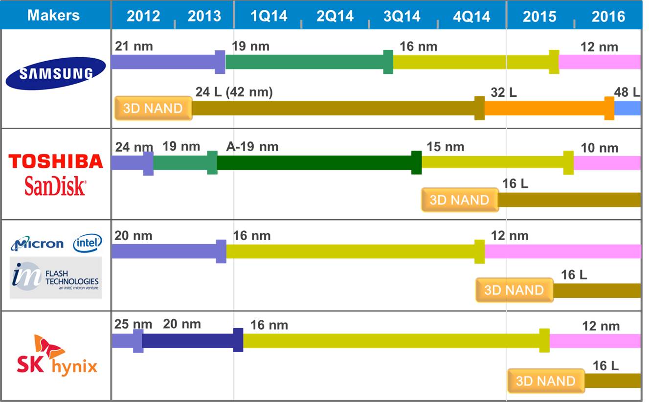
Here’s the current technology roadmap for NAND flash courtesy of my friends at TechInsights:
Technology Roadmap for NAND Flash (Image courtesy of TechInsights)
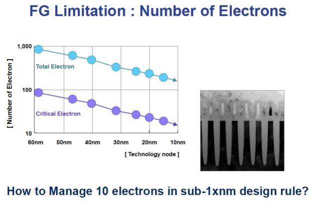
So what’s the problem with flash getting smaller? Well, hopefully for the very last time, cast your mind back to the concept of floating gate transistors. On these tiny devices the floating gates effectively capture and store electrons that are passing from one side of the transistor to another, retaining charge – and that charge determines the cell’s value of 0 or 1. But at the tiny geometries that flash is approaching now, the number of electrons involved is desperately small, resulting in large margins for error. Electrons, after all, are notoriously good at hide and seek.
Floating Gate Limitations (SK Hynix Presentation – Aug 2012)
This means that flash cells are less reliable, that even more error correction codes are required… and that ultimately, we are reaching what is known as the scaling limit. It looks like the end is it sight for flash as we know it.
3D NAND Flash
Except it isn’t. If you look again at the Technology Roadmap picture you’ll see entries appearing alongside each foundry operator for 3D NAND. This is a significant new fabrication process that looks like it will be the direction taken by the flash industry for the foreseeable future. I would love to attempt a detailed explanation of 3D NAND design here, but a) it’s beyond me, b) I promised to listen to the feedback after the last time I went sub-atomic, and c) Jim Handy (AKA The Memory Guy) already has a fantastic set of articles all about it.
The point is, 3D NAND maps out a future for NAND flash beyond the scaling limits of 2D planar NAND – and the big fab operators have already invested. That puts 3D NAND in pole position as we increasingly look to non-volatile memory to store our data.
But there are other technologies trying to compete…
The Next Big Thing
The holy grail of memory technology is universal memory. This is a hypothetical technology which brings all the benefits, but none of the drawbacks, of the multitude of memory technologies in use today: SRAM, DRAM, NAND Flash and so on. SRAM (often used on-chip as a CPU cache) is fast but expensive, DRAM is cheaper but must be constantly refreshed (using considerably more power) while NAND flash is comparatively slower and wears out with use. If only there were some new technology that met all our requirements?
Well, first of all, it’s worth mentioning that if universal memory did come about it would have far-reaching consequences on the way we design and build computers… but all the same, there are various technologies in R&D right now which make claims to be the NVM solution of the future: PCM, MRAM, RRAM, FeRAM, Memristor and so on. But these – and any other – technologies all face the same challenge: that massive initial investment required to go from prototype to production. In other words, the cost and time associated with building a fabrication plant.
R&D Centre for SHRAM
Say you converted your shed into a clean room and invented a wonderful new memory technology called Shed-RAM (SHRAM). SHRAM is fast, cheap, dense and only uses a tiny amount of power. You’ve still got to convince somebody to splurge billions of dollars on a foundry before it can be productised. And, as I’m sure you’ll agree, that’s a pretty big bet on an untested technology – especially if it takes years to build. What happens if, one year in, your neighbour (who recently converted his garage into a clean room) invents Garage-RAM (GaRAM) which makes your SHRAM worthless? Nobody is going to cope well with the loss of billions of dollars on a bad bet.
Conclusion
The investment hurdle required to turn a new NVM technology into a product is both a challenge and a stabiliser to the NVM industry. In theory it could stifle potential new technologies, but at the same time (at least for those of us in enterprise storage) it means there is plenty of warning when the tide turns: you are likely to see any successful new tech in your phone before it appears in your data centre.
Now, who can lend me $15 billion to build a new fab? I can’t afford anything more than 0% interest, but I can offer a lifetime’s supply of USB sticks to sweeten the deal…
Storage architecture shapes database behaviour – and that relationship is evolving again. If you found this series useful, you might also be interested in Databases in the Age of AI, which explores how AI agents are changing the assumptions at the heart of enterprise data systems.
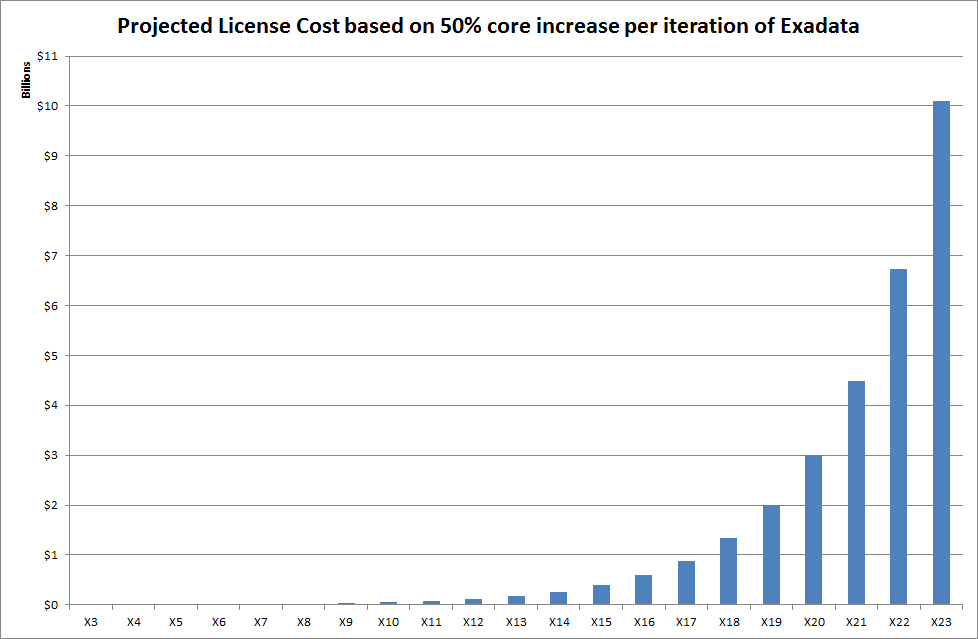
Now that the dust has settled on the announcement of Oracle’s new Exadata X5 Database Machine, I’ve been doing some research in order to update my History of Exadata post (it’ll be ready soon). While reviewing the datasheets and other collateral for the X5 I was struck by the meteoric increase in one particular statistic: the number of processor cores on each database server. Oracle is riding that Moore’s Law train all the way to the bank.
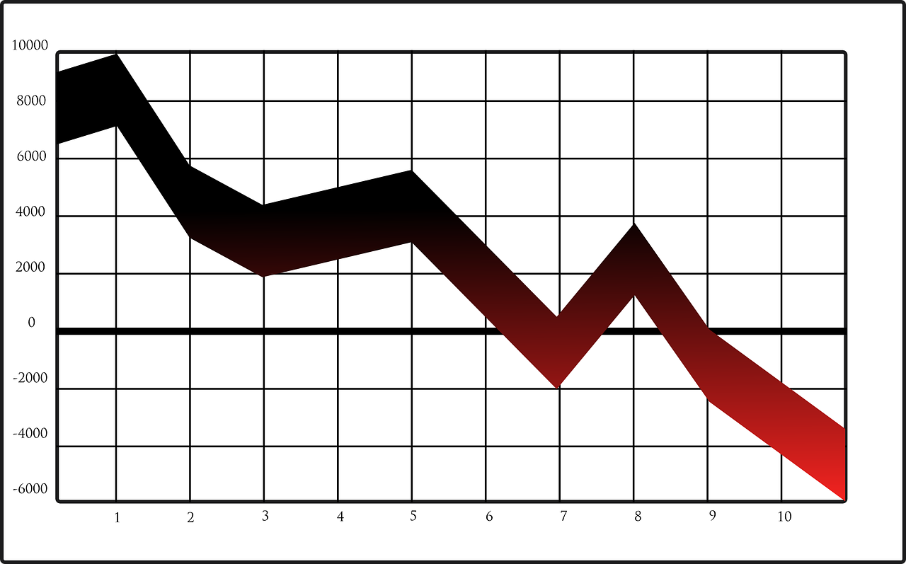
The thing is, the number of cores per database server is directly linked to the cost of licensing the Oracle Database for each Exadata machine – and that means trouble if you are the one paying the bills. Assuming you buy a full rack – and that you license every core in every database server (which is the most common choice, since only a very brave minority would consider the Oracle VM Trusted Partitions option), your license cost has been increasing by 50% for each of the last two Exadata releases (X3-2 to X4-2 to X5-2). Let’s have a look at that in graphical form (click on the image to enlarge):
Let’s not forget here that I am only plotting the cost of licensing the database software. We are not taking into account the extra costs associated with paying for the hardware, licensing the storage servers or purchasing any of the pretty-much essential enterprise edition options such as Oracle RAC, partitioning, multitenancy or the diagnostic pack license. Nor are we considering the infamous 22% per annum software support costs. I’m also using the list price – which you would never expect to pay – but even if you used discounted prices the percentage increases would remain the same.
Anyway, after crunching the numbers it turns out there is good news and bad news…
Good News for Oracle
The good news for Oracle is that if Exadata continues to increase the number of cores at the rate of 50% extra per release, the list price for licensing the database software on the future X23-2 model will be $10.1 billion:
There’s no doubt about it – this will pay for a lot of yachts.
Bad News for Oracle
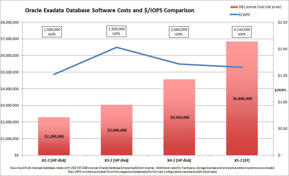
There is a downside though. As Kevin Closson has already shown, Oracle appears to be having trouble balancing the I/O capabilities of the X5 against this tremendously-increased compute power. Even after abandoning previous claims that a memory hierarchy with “low-cost disk” as the bottom tier would bring the “highest performance at the lowest cost” to customers, the new Oracle Exadata X5 “Extreme Flash” model (because apparently flash on its own isn’t enough, it has to be extreme flash) struggles to deliver an improvement in IOPS per flash device, as Kevin has shown.
Excerpt from the Oracle Exadata X5-2 Press Release
You wouldn’t think this from reading the press release, which promises “breakthrough performance and price per I/O” (emphasis added by me). Price per I/O, eh? That sounds like we take the overall price and divide it by the number of IOPS the system can deliver, right?
So let’s do that. And to be generous, let’s only look at the database license cost (ignoring all those other costs again) and take the maximum IOPS number from the datasheets (which in most cases is for unrealistic, 100% read only, fully cached workloads). How will it look? I’ll overlay it as a line (in blue) on top of the first graph:
Well it turns out that the price per I/O is actually falling: it’s down from $1.71 on the X4-2 (HP) model to $1.65 on the X5-2 EF. But three and a half percent is not much of an improvement considering the 50% extra on the price tag, is it? And as for offering a “breakthrough” price per I/O, the X2-2 was better at only $1.52 per I/O per second!
Summary
In my view, something is not right about the balance between compute and storage on the Exadata X5. It feels as though Oracle is bumping up the compute power faster than would be architecturally prudent because this results in a higher purchase price. Maybe I’m wrong – I have no insider knowledge and can only speculate… but when the Exadata X23-2 finally comes out in a couple of decades time, maybe we’ll know for sure.
Footnote
The comments section of this article makes for interesting reading, with responses from a number of Oracle employees – although not necessarily speaking on behalf of the mothership. The noteworthy (not to mention calm and measured) comments come from the Exadata Product Manager, Gurmeet Goindi. In addition I’d like to draw your attention to the following two URLs:
Back in July 2013, Oracle released the latest version of its flagship database product, Oracle 12c. Among the usual fanfare was information about a number of new options – including one known as Multitenant. With the Multitenant option, databases use a new architecture which features a container database (or CDB) which in turn contains one or more pluggable databases (or PDBs). Use of Multitenant requires a licence – which at the time of writing retails at $17,500 per processor (perpetual) plus 22% per annum for support.
This post is not intended to discuss the way Multitenant works – if you want to read more about it, Tim has a great set of articles about Multitenant here. But keep in mind that you can choose to install the Multitenant feature or not. If you do install it, you can create a single PDB within your CDB without requiring the license. As soon as you use more than one PDB the license is required.
What I want to talk about is Oracle’s attitude to its customers and what seems to me to be breathtaking arrogance. Personally I can think of three very good reasons why I might not want to use the single PDB within a CDB configuration which does not require a Multitenant license:
Multitenant requires additional configuration and the use of new administrative commands, which means re-writing admin procedures and re-training operations staff
Multitenant is an entirely new feature, with new code paths – which means it carries a risk of bugs (the list of bug fixes for the 12.1.0.2 patchset contains a section on Pluggable/Container Databases which lists no fewer than 105 items)
With the Multitenant option installed it is possible to trigger the requirement for an expensive set of licenses due to human error… without the option installed this is not possible
So it seems to me that, while Multitenant might be an interesting and useful new feature to evaluate, it is not something that I would want to be forced into using on production environments just yet. As always, people who manage production environments are conservative in their attitude to risk.
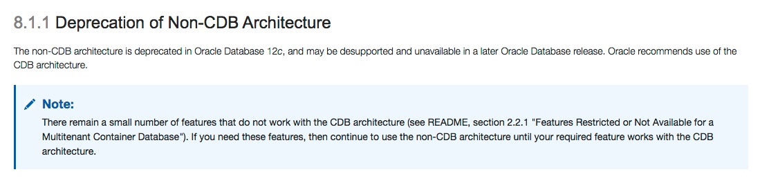
The non-CDB architecture (i.e. the old way of building a database without CDBs and PDBs) has been deprecated in 12c and “may be desupported or unavailable” in later releases of Oracle Database. In other words, you need to change to using the CDB and PDB configuration now, even if you do not plan to purchase the Multitenant option.
It would be nice to have the choice, wouldn’t it?
Deprecated versus Desupported
OK so first let’s just remember that the term deprecated does not mean the same as the term desupported. We can dip back into the documentation to define these two important terms:
“By deprecate, we mean that the feature is no longer being enhanced but is still supported for the full life of the 12.1 release. By desupported, we mean that Oracle will no longer fix bugs related to that feature and may remove the code altogether.”
– Oracle Database 12c Upgrade Guide
It seems that Oracle will still support the use of non-CDB databases and will continue to do so for the lifetime of the 12.1 release. But, if you were designing a new system right now, it would take some confidence to choose a configuration which is deprecated and already living on death row.
And there’s more. The deprecation notice says there are some features that still do not work with the CDB architecture – and that if you want to use these you should use the deprecated non-CDB architecture. The list of features which are restricted or not available includes Automatic Data Optimization, Heat Maps, DBVERIFY and Flashback Pluggable Database (you can see the complete lists here for 12.1.0.1 and 12.1.0.2).
So we can add a fourth reason to our list of three drawn up earlier:
The Multitenant causes a number of other options or features to be unusable
Now, given that I think all four reasons stated here are good enough to stand up on their own, what does this say about Oracle’s decision to deprecate non-CDB architectures?
You can draw your own conclusion, but I can’t help see it as arrogance on Oracle’s part as they force customers to use a specific new configuration with little regard for how it affects their operations. At worst, I don’t like being forced into changes by the vendor (to whom customers pay large amounts of money) while at best I would at least expect them to get all the features working before forcing the issue…
Update – 18 February 2015
Since I published this article back in late January I’ve had a lot of comments – both here and on Twitter. Some agree with me, some disagree – and unsurprisingly many of the latter are Oracle employees. One particular Oracle employee took to his corporate blog to post a four-part response!
One of those responses was in regard to my concern that, since it seemingly cannot be unlinked, customers may be able to inadvertently trigger usage of the Multitenant feature and thus incur an expensive and unexpected license bill. [I have no knowledge that this has ever happened, I am merely concerned that it may be possible.]
I’d like to quote the following response from our friend on the Oracle blog (his own opinion, not the views of his employer) who is apparently looking to rubbish that concern. I have placed the most enlightening part of the text in bold for emphasis:
This bit of FUD is silly. First of all, this risk already exists with various features of the Oracle database. For example, many of the OEM packs can be inadvertently used without a license as could several of the views in the database itself. Partitioning is another example that comes to mind. Often it’s installed in a database but it’s use requires a license.
So, how is this any different? Well, it’s not. Simply put, this is an argument for enterprise compliance auditing/management.
I hope this convinces you more than it convinces me.


 Flash for DBAs: A new technology is sweeping the world of storage. Flash, a type of non-volatile memory, is gradually replacing hard disk drives. It began in consumer electronic devices such as phones, cameras and tablets – then it moved into laptops in the form of SSDs. And now the last fortress of hard drives us under attack: the data centre. Find out what flash memory is, what it means for your Oracle databases and how to use it to give you performance that was never possible in the old days of disk…