Why Kaminario?

K2-mountain

This summer I made the decision to leave my previous employer and join another vendor in the All Flash Array space – a company called Kaminario. A lot of people have been in touch to ask me about this, so I thought I’d answer the question here… Why Kaminario?

To answer the question, we first need to look at where the All Flash industry finds itself today…

The Path To Flash Adoption

We all know that disk-based storage has been struggling to deliver to the enterprise for many years now. And most of us are aware that flash memory is the technology most suitably placed to take over the mantle as the storage medium of choice. However, even keeping in mind the typical five-to-seven year refresh cycle for enterprise storage platforms, the journey to adopt flash in the enterprise data centre has been slower than some might have expected. Why?

There are three reasons, in my view. The first two are pretty obvious: cost and functionality. I’ll cover the third in another post – but cost and functionality have changed drastically over the four phases of flash:

Phase One: Extreme Performance

The early days of enterprise flash storage were pioneered by the likes of FusionIO with their PCIe flash cards. These things sold for a $/GB price that would seem obscene in today’s AFA marketplace – and (at least initially) Fusion-io-ioDrive-Duo-640GBthey had almost no functionality in terms of thin provisioning, replication, snapshots, data reduction technologies and so on. They weren’t even shared storage! They were just fast blobs of flash that you could stick right inside your server to get performance which, at the time, seemed insanely fast – think <250 microseconds of latency.

This meant they were only really suitable for extreme performance requirements, where the cost and complexity was justified by the resultant improvement to the application.

Phase Two: Niche Performance Applications

Violin 6000 series flash memory arrayThe next step on the path to flash adoption was the introduction of flash as shared storage (i.e. SAN). These were the first All Flash Arrays, a marketplace pioneered by Violin Memory (my former employer) and Texas Memory Systems (subsequently acquired by IBM). The fact that they were shared allowed a larger number of applications to be migrated to flash, but they were still very much used as a niche performance play due to a lack of features such as data reduction, replication etc.

Phase Three: Virtualization for Servers and Desktops

The third phase was driven by the introduction of a very important feature: data reduction. Pure StorageBy implementing deduplication and/or compression – therefore massively reducing the effective price in $/GB – a couple of new entrants to the AFA space were able to redefine the marketplace and leave the pioneering AFA vendors floundering. These new players were Pure Storage and EMC with its XtremIO system – and they were able to create and attack an entirely new market: virtualization. Initially they went after Virtual Desktop Infrastructure projects, which have lots of duplicate data and create lots of IOPS, but in time the market for Virtual Server Infrastructure (i.e. VMware, Hyper-V, Xen etc) became a target too.

Phase Four: General Purpose Storage

This is where we are now – or at least, it’s where we’ve just arrived. The price of flash storage has consistently dropped as the technology has advanced, while almost all of the features and functionality originally found on enterprise-class disk arrays are now available on AFAs. We’re finally at the point now where, with some caveats, customers are either moving to or planning the wholesale replacement of their general purpose disk arrays with All Flash. Indeed, with the constant evolution of NAND flash technology it’s no longer fanciful to believe that Backup and Archive workloads could also move to flash…

We are now at the inflection point where, thanks to the combination of data reduction features and constantly-evolving NAND flash development, the cost of All Flash storage has fallen as low as enterprise disk storage while delivering all the functionality required to replace disk entirely. We call this concept the All-Flash Data Centre.

So to answer the question at the start of this post, I have joined Kaminario because I believe they are ideally placed, architecturally and commercially, to lead the adoption of this new phase of flash storage – a technology that I fundamentally believe in.

Making The All-Flash Data Centre A Reality

iphoneI mentioned earlier that NAND flash is changing and evolving all the time. It reminds me a little of smartphones – you buy the latest and greatest model only for it to become yesterday’s news almost before you’ve worked out how to use it. But the typical refresh cycle of a smartphone is one-to-two years, while for enterprise storage it’s five-to-seven. That’s a long time to risk an investment in evolving technology.

Kaminario’s K2 All Flash Array is based on its SPEAR architecture. Essentially, what Kaminario has created is a high-performance, scalable framework for taking memory and presenting it as enterprise-class storage – with all Kaminario's SPEAR architecturethe resilience, functionality and performance you would expect. When the company was first founded this memory was just that: DRAM. But since NAND flash became economically viable, Kaminario has been using flash – and the architecture is agile enough to adopt whichever technology makes the most sense in the future.

As an example of this agility, Kaminario was the first AFA vendor to adopt 3D NAND technology and the first to adopt 3D TLC. This obviously allows a major competitive advantage when it comes to providing the most cost-efficient All Flash Array. But what really drew me to Kaminario was their decision to allow customers to integrate future hardware (such as new types of flash) into their existing arrays rather than making them migrate to a new product as is typical in the industry. By protecting customers’ investments, Kaminario is taking some of the risk out of moving to an AFA solution. It calls this programme the Perpetual Array.

In addition to this, Kaminario has a unique ability to offer both scale out and scale up architecture (scalability is something I will discuss further in my Storage for DBAs series soon) and to deliver workload agnostic performance… all technical features that deliver real business value. But those are for discussion another day.

For today the message is simple: Kaminario is making the All Flash Data Centre a reality.. and I want to be here to help customers make that happen.

All Flash Arrays: SSD-based versus Ground-Up Design

design-papers

In recent articles in this series I’ve been looking at the architectural choices for building All Flash Arrays (AFAs). I surmised that there are three main approaches:

  • Hybrid Flash Arrays
  • SSD-based All Flash Arrays
  • Ground-Up All Flash Arrays (which from here on I’ll refer to as Custom Flash Module arrays or CFM arrays)

I’ve already blown metaphorical raspberries at the hybrid approach, so now it’s time to cover the other two.

SSD or CFM: The Big Question

I think the most interesting question in the AFA industry right now is the one of whether the SSD or CFM design will win. Of course, it’s easy to say “win” like that as if it’s a simple race, but this is I.T. – there’s never a simple answer. However, the reality is that each method offers benefits and drawbacks, so I’m going to use this blog post to simply describe them as I see them.

Before I do that, let me just remind you of what the vendor landscape looks like at this time:

SSD-based architecture: Right now you can buy SSD-based arrays from EMC (XtremIO), Pure Storage, Kaminario, Solidfire, HP 3PAR and Huawei to name a few. It’s fair to say that the SSD-based design has been the most common in the AFA space so far.

CFM-based architecture: On the other hand, you can now buy ground-up CFM-based arrays from Violin Memory, IBM (FlashSystem), HDS (VSP), Pure Storage (FlashArray//m) and EMC (DSSD). The latter has caused some excitement because of DSSD’s current air of mystery in the marketplace – in other words, the product isn’t yet generally available.

So which approach is “the best”?

The SSD-based Approach

If you were going to start an All Flash Array company and needed to bring a product to market as soon as possible, it’s quite likely you would go down the SSD route. Apart from anything else, flash management is hard work – and needs constant attention as new types of flash come to market. A flash hardware engineer friend of mine used to say that each new flash chip is like a snowflake – they all behave slightly differently. So by buying flash in the ready-made form of an SSD you bypass the requirement to put in all this work. The flash controller from the SSD vendor does it for you, leaving you to concentrate on the other stuff that’s needed in enterprise storage: resilience, availability, data services, etc.Samsung_840_EVO_SSD

On the other hand, it seems clear that an SSD is a package of flash pretending to behave like a disk. That often means I/Os are taking place via protocols that were designed for disk, such as Serial Attached SCSI. Also, in a unit the size of an all flash array there are likely to be many SSDs… but because each one is an isolated package of flash, they cannot work together and manage the flash holistically. In other words, if one SSD is experiencing issues due to garbage collection (for example), the others cannot take the strain.

The Ground-Up Approach

For a number of years I worked for Violin Memory, which adopted the ground-up approach at its very core. Violin’s position was that only the CFM approach could unlock the full potential benefits from NAND flash. By tightly integrating the NAND flash into its array – and by using its own controllers to manage that flash – Violin believed it could deliver the best performance in the AFA market. On the other hand, many SSD vendors build products for the consumer market where the highest levels of performance simply aren’t necessary. All that’s required is something faster than disk – it doesn’t always have to be the fastest possible solution.electronics

It could also be argued that any CFM vendor who has a good relationship with a flash fabricator (for example, Violin was partly-owned by Toshiba) could gain a competitive advantage by working on the very latest NAND flash technologies before they are available in SSD form. What’s more, SSDs represent an additional step in the process of taking NAND flash from chip to All Flash Array, which potentially means there’s an extra party needing to make their margin. Could it be that the CFM approach is more cost effective? [Update from Jan 2017: Violin Memory has now filed for chapter 11 bankruptcy protection]

SSD Economics

The argument about economics is an interesting one. Many technical people have a tendency to focus on what they know and love: technology. I’m as guilty of this as anyone – given two solutions to a problem I tend to gravitate toward the one that has the most elegant technical design, even if it isn’t necessarily the most commercially-favourable. Taking raw flash and integrating it into a custom flash module sounds great, but what is the cost of manufacturing those CFMs?

moneyManufacturing is all about economies of scale. If you design something and then build thousands of them, it will obviously cost you more per unit than if you build millions of them. How many ground-up all flash vendors are building their custom flash modules by the millions? In May 2015, IBM issued this press release in which they claimed that they were the “number one all-flash storage array vendor in 2014“. How many units did they ship? 2,100.

In just the second quarter of 2015, almost 24 million SSDs were shipped to customers, with Samsung responsible for 43.8% of that total (according to US analyst firm Trendfocus, Inc). Who do you think was able to achieve the best economy of scale?

Design Agility

The other important question is the one about New Stuff ™. We are always being told about fantastic new storage technologies that are going to change our lives, so who is best placed to adopt them first?

Again there’s an argument to be made on both sides. If the CFM flash vendor is working hand-in-glove with a fabricator, they may have access to the latest technology coming down the line. That means they can be prepared ahead of the pack – a clear competitive advantage, right?

But how agile is the CFM design? Changing the NVM media requires designing an entirely-new flash module, with all the associated hardware engineering costs such as prototyping, testing, QA and limited initial manufacturing runs.

For an SSD all flash array vendor, however, that work is performed by the SSD vendor… again somebody like Samsung, Intel or Micron who have vast infrastructures in place to perform that sort of work all the time. After all, a finished SSD must behave exactly like a disk, regardless of what NVM technology it uses under the covers.

Conclusion

There are obviously two sides to this argument. The SSD was designed to replace a fundamental bottleneck in storage systems: the hard disk drive. Ironically, it may be the fate of the SSD to become exactly what it replaced. For flash to become mainstream it was necessary to create a “flash-behaving-as-disk” package, but the flip side of this is the way that SSDs stifle the true potential of the underlying flash. (Although perhaps NVMe technologies will offer us some salvation…)question-mark-dice

However, unless you are a company the size of Samsung, Intel or Micron it seems unlikely that you would be able to retain the manufacturing agility and economies of scale required to produce custom flash modules at the price point of SSDs. Nor would you be likely to have the agility to adopt new NVM technologies at the moment that they become economically preferable to whatever medium you were using previously.

Whatever happens, you can be sure that each side will claim victory. With the entire primary data market to play for, this is a high stakes game. Every vendor has to invest a large amount of money to enter the field, so nobody wants to end up being consigned to the history books as the Betamax of flash…

For younger readers, Betamax was the loser in a battle with VHS over who would dominate the video tape market. You can read about it here. What do you mean, “What is a video tape?” Those things your parents used to watch movies on before the days of DVDs. What do you mean, “What is a DVD?” Jeez, I feel old.

All Flash Arrays: Where’s My Capacity? Effective, Usable and Raw Explained

capacity-effective-usable-raw

What’s the most important attribute to consider when you want to buy a new storage system? More critical than performance, more interesting than power and cooling requirements, maybe even more important than price? Whether it’s an enterprise-class All Flash Array, a new drive for your laptop or just a USB flash key, the first question on anybody’s mind is usually: how big is it?

Yet surprisingly, at least when it comes to All Flash Arrays, it is becoming increasingly difficult to get an accurate answer to this question. So let’s try and bring some clarity to that in this post.

Before we start, let’s quickly address the issue of binary versus decimal capacity measurements. For many years the computer industry has lived with two different definitions for capacity: memory is typically measured in binary values (powers of two) e.g. one kibibyte = 2 ^ 10 bytes = 1024 bytes. On the other hand, hard disk drive manufacturers have always used decimal values (powers of ten) e.g. one kilobyte = 10 ^ 3 bytes = 1000 bytes. Since flash memory is commonly used for the same purpose as disk drives, it is usually sold with capacities measured in decimal values – so make sure you factor this in when sizing your environments.

Definitions

Now that’s covered, let’s look at the three ways in which capacity is most commonly described: raw capacity, usable capacity and effective capacity. To ensure we don’t stray from the truth, I’m going to use definitions from SNIA, the Storage Networking Industry Association.

Raw Capacity: The sum total amount of addressable capacity of the storage devices in a storage system.

rawThe raw capacity of a flash storage product is the sum of the available capacity of each and every flash chip on which data can be stored. Imagine an SSD containing 18 Intel MLC NAND die packages, each of which has 32GB of addressable flash. This therefore contains 576GB of raw capacity. The word addressable is important because the packages actually contain additional unaddressable flash which is used for purposes such as error correction – but since this cannot be addressed by either you or the firmware of the SSD, it doesn’t count towards the raw value.

Usable Capacity: (synonymous with Formatted Capacity in SNIA terminology) The total amount of bytes available to be written after a system or device has been formatted for use… [it] is less than or equal to raw capacity.

usablePossibly one of the most abused terms in storage, usable capacity (also frequently called net capacity) is what you have left after taking raw capacity and removing the space set aside for system use, RAID parity, over-provisioning (i.e. headroom for garbage collection) and so on. It is guaranteed capacity, meaning you can be certain that you can store this amount of data regardless of what the data looks like.

That last statement is important once data reduction technologies come into play, i.e. compression, deduplication and (arguably) thin provisioning. Take 10TB of usable space and write 5TB of data into it – you now have 5TB of usable capacity remaining. Sounds simple? But take 10TB of usable space and write 5TB of data which dedupes and compresses at a 5:1 ratio – now you only need 1TB of usable space to store it, meaning you have 9TB of usable capacity left available.

Effective Capacity: The amount of data stored on a storage system … There is no way to precisely predict the effective capacity of an unloaded system. This measure is normally used on systems employing space optimization technologies.

effectiveThe effective capacity of a storage system is the amount of data you could theoretically store on it in certain conditions. These conditions are assumptions, such as “my data will reduce by a factor of x:1”. There is much danger here. The assumptions are almost always related to the ability of a dataset to reduce in some way (i.e. compress, dedupe etc) – and that cannot be known until the data is actually loaded. What’s more, data changes… as does its ability to reduce.

For this reason, effective capacity is a terrible measurement on which to make any firm plans unless you have some sort of guarantee from the vendor. This takes the form of something like, “We guarantee you x terabytes of effective capacity – and if you fail to realise this we will provide you with additional storage free of charge to meet that guarantee”. This would typically then be called the guaranteed effective capacity.

The most commonly used assumptions in the storage industry are that databases reduce by around 2:1 to 4:1, VSI systems around 5:1 to 6:1 and VDI systems anything from 8:1 right up to 18:1 or even further. This means an average data reduction of around 6:1, which is the typical ratio you will see on most vendor’s data sheets. If you take 10TB of usable capacity and assume an average of 6:1 data reduction, you therefore end up with an effective capacity of 60TB. Some vendors use a lower ratio, such as 3:1 – and this is good for you the customer, because it gives you more protection from the risk of your data not reducing.

But it’s all meaningless in the real world. You simply cannot know what the effective capacity of a storage system is until you put your data on it. And you cannot guarantee that it will remain that way if your data is going to change. Never, ever buy a storage system based purely on the effective capacity offered by the vendor unless it comes with a guarantee – and always consider whether the assumed data reduction ratio is relevant to you.

Think of it this way: if you are being sold effective capacity you are taking on the financial risk associated with that data reduction. However, if you are being sold guaranteed effective capacity, the vendor is taking on that financial risk instead. Which scenario would you prefer?

Use and Abuse of Capacities

Three different ways to measure capacity? Sounds complicated. And in complexity comes opportunities for certain flash array vendors to use smoke and mirrors in order to make their products seem more appealing. I’m going to highlight what I think are the two most common tactics here.

1. Confusing Usable Capacity with Effective Capacity

Many flash array vendors have Always-On data reduction services. This is often claimed to be for the customer’s benefit but is often more about reducing the amount of writes taking place to the flash media (to alleviate performance and endurance issues). For some vendors, not having the ability to disable data reduction can be spun around to their advantage: they simply make out that the terms usable and effective are synonymous, or splice them together into the unforgivable phrase effective usable capacity to make their products look larger. How convenient.

Let me tell you this now: every flash array has a usable capacity… it is the maximum amount of unique, incompressible data that can be stored, i.e. the effective capacity if the data reduction ratio were 1:1. I would argue that this is a much more important figure to know when you buy a flash system, because if you buy on effective capacity you are just buying into dreams. Make your vendor tell you the usable capacity at 1:1 data reduction and then calculate the price per GB based on that value.

2. My Data Reduction Is Better Than Yours

Every flash vendor thinks their data reduction technologies are the best. They can’t all be right. Yet sometimes you will hear claims so utterly ridiculous that you’ll think it’s some kind of joke. I guess we all believe what we want to hear.

Here’s the truth. Compression and deduplication are mature technologies – they have been around for decades. Nobody in the world of flash storage is going to suddenly invent something that is remarkably better than the competition. Sometimes one vendor’s tech might deliver better results than another, but on other days (and, crucially, with other datasets) that will reverse. For this reason, as well as for your own sanity, you should assume they will all be roughly the same… at least until you can test them with your data. When you evaluate competitive flash products, make them commit to a guaranteed effective capacity and then hold them to it. If they won’t commit, beware.

3. Including Savings From Thin Provisioning

Thin Provisioning is a feature whereby physical storage is allocated only when it is used, rather than being preallocated at the moment of volume creation. Thus if a 10TB volume is created and then 1TB of data written to it, only 1TB of physical storage is used. The host is fooled into thinking that it has all 10TB available, but in reality there may be far less physical capacity free on the storage system.

Some vendors show the benefits from thin provisioned volumes as a separate saving from compression and deduplication, but some roll all three up into a single number. This conveniently makes their data reduction ratios look amazing – but in my opinion this then becomes a joke. Thin provisioning isn’t data reduction, because no data is being reduced. It’s a cheap trick – and it says a lot about the vendor’s faith in their compression and deduplication technologies.

Conclusion

Don’t let your vendors set the agenda when it comes to sizing. If you are planning on buying a certain capacity of flash, make sure you know the raw and usable capacities, plus the effective capacity and the assumed data reduction ratio used to calculate it. Remember that usable should be lower than raw, while effective (which is only relevant when data reduction technologies are present) will commonly be higher.

Keep in mind that Effective Capacity = Usable Capacity X Data Reduction Factor.

Be aware that when a product with an “Always-On” data reduction architecture tells you how much capacity you have left, it’s basically a guess. In reality, it’s entirely dependent on the data you intend to write. I’ve always thought that “Always-On” was another bit of marketing spin; you could easily rename it as an “Unavoidable” or “No Choice” architecture.

In my opinion, the best data reduction technology will be selectable and granular. That means you can choose, at a LUN level, whether you want to take advantage of compression and/or deduplication or not – you aren’t tied in by the architecture. Like with all features, the architecture should allow you to have a choice rather then enforce a compromise.

Finally, remember the rule about effective capacity. If it’s guaranteed, the risk is on the vendor. If they won’t guarantee, the risk is on you.

So there we have it: clarity and choice. Because in my opinion – and no matter which way you measure it – one size simply doesn’t fit all.

All Flash Arrays: Can’t I Just Stick Some SSDs In My Disk Array?

dinosaur-velociraptor

In the previous post of this series I outlined three basic categories of All Flash Array (AFA): the hybrid AFA, the SSD-based AFA and the ground-up AFA. This post addresses the first one and is therefore aimed at answering one of the questions I hear most often: why can’t I just stick a bunch of SSDs in my existing disk array?

Data Centre Dinosaurs

Disk arrays – and in this case we are mainly talking about storage area networks – have been around for a long time. Every large company has a number of monolithic, multi-controller cache-based disk arrays in their data centre. They are the workhorses of storage: ever reliable, able to host multiple, mixed workloads and deliver predictable performance. Predictably slow performance, of course – but you mustn’t underestimate just how safe these things feel to the people who are paid to ensure the safety of their data. Add to this the full suite of data services that come with them (replication, mirroring, snapshots etc) and you have all that you could ask for.

Battleship!

Battleship!

Except of course that they are horribly expensive, terribly slow and use up vast amounts of power, cooling and floor space. They are also a dying breed, memorably described by Chris Mellor of The Register as like outdated battleships in an era of modern warfare.

The SSD Power-Up

Every large vendor has a top-end product: EMC’s VMAX, IBM’s DS8000, HDS’s VSP… and pretty much every product has the ability to use SSDs in place of disk drives. So why not fill one of these monsters with flash drives and then call it an “All Flash Array”? Just like in those computer games where your spacecraft hits a power-up and suddenly it’s bigger and faster with better weapons… surely a bunch of SSDs would convert your ageing battleship into a modern cruiser with new-found agility and seaworthiness. Ahoy! [Ok, I’ll stop with the naval analogies now]

Well, no. And to understand why, let’s look at how most disk arrays are architected.

The Classic Disk Array Architecture

Let’s consider what it takes to build a typical SAN disk array. We’ll start with the most obvious component, which is the hard disk drive itself. These things have been around for decades so we are fairly familiar with them. They offer pretty reasonable capacity of up to 4TB (in fact there are even a few 6TB models out now) but they have a limitation with regard to performance: you are unlikely to be able to drive much more than 200 transactions per second.

At this point, stop and think about the performance characteristics of a hard disk drive. Disks don’t really care if you are doing read or write I/Os – the performance is fairly symmetrical. However, there is a drastic difference in the performance of random versus sequential I/Os: each I/O operation incurs the penalty of latency. A single, large I/O is therefore much more efficient than many, small I/Os.

This is the architectural constraint of every hard disk drive and therefore the design challenge around which we much architect our disk array.

In the next section we’re going to build a disk array from scratch, considering all the possibilities that need to be accounted for. If it looks like it will take too long to read, you can skip down to the conclusion section at the end.

Building A Disk Array

We’re now going to build a disk array, so the first ingredient is clearly going to be hard drives. So let’s start by taking a bunch of disks and putting them into a shelf, or some other form of enclosure:

build-a-disk-array1

At this point the density is limited by the number of disks we can fit into the enclosure, which might typically be 25 if they are of the smaller form factor or up to around 14 if they are the larger 3.5 inch variety.

Next we’re going to need a controller – and in that controller we’re going to want a large chunk of DRAM to act as a cache in order to try and minimise the number of I/Os hitting the disk enclosure. We’ll allocate some of that DRAM to work as a read cache, in the hope that many of the reads will be hitting a small subset of the data stored, i.e. the “hot” blocks. If this gamble is successful we will have taken some load off of the disks – and that is a Good Thing:

build-a-disk-array2

The rest of the DRAM will be allocated to a write cache, because clearly we don’t want to have to incur the penalty of rotational latency every time a write I/O is performed. By writing the data to the DRAM buffer and then issuing the acknowledgement back to the client, we can take our time over writing the data to the persistent storage in the disk enclosure.

Now, this is an enterprise-class product we are trying to build, so that means there are requirements for resiliency, redundancy, online maintenance etc. It therefore seems pretty obvious that having only one controller is a single point of failure, so let’s add another one:

build-a-disk-array3

This brings up a new challenge concerning that write cache we just discussed. Since we are acknowledging writes when they hit DRAM it could be possible for controller to crash before changed blocks are persisted to disk – resulting in data loss. Also, an old copy of a block could be in the cache of one controller while a newly-changed version exists in the other one. These possibilities cannot be allowed, so we will need to mirror our write cache between the controllers. In this setup we won’t acknowledge the write until it’s been written to both write caches.

Of course, this introduces a further delay, so we’ll need to add some sort of high speed interconnect into the design to make the process of mirroring as fast as possible:

build-a-disk-array4

This mirroring may protect us from losing data in the event of a single controller failure, but what about if power to the entire system was lost? Changed blocks in the mirrored write cache would still be lost, resulting in lost data… so now we need to add some batteries to each controller in order to provide sufficient power that cached writes can be flushed to persistent media in the event of any systemic power issue:

build-a-disk-array5

That’s everything we need from the controllers – so now we need to connect them together with the disks. Traditionally, disk arrays have tended to use serial architectures to attach disks onto a back end network which essentially acts as a loop. This has some limitations in terms of performance but when your fundamental building blocks are each limited to 200 IOPS it’s hardly the end of the world:

build-a-disk-array6

So there we have it. We’ve built a disk array complete with redundant controllers and battery-backed DRAM cache. Put a respectable logo on the front and you will find this basic design used in data centres around the world.

But does it still make sense if you switch to flash?

From HDD To SSD

Let’s take our finished disk array design and replace the disks with SSDs:

build-a-disk-array7

And now let’s take a moment to consider the performance characteristics of flash: the latency is much lower than disk, meaning the penalty for performing random I/Os instead of sequential I/Os is negligible. However, the performance of read versus write I/Os is asymmetrical: writes take substantially longer than reads – especially sustained writes. What does that do to all of the design principles in our previous architecture?

  • With so many more transactions per second available from the SSDs, it no longer makes sense to use a serial / loop based back end network. Some sort of switched infrastructure is probably more suitable.
  • Because the flash media is so much faster than disk (i.e. has a significantly lower latency), we can do away with the read cache. Depending on our architecture, we may also be able to avoid using a write cache too – resulting in complete removal of the DRAM in those controllers (although this would not be the case if deduplication were to be included in the design – more on that another time).
  • If we no longer have data in DRAM, we no longer need the batteries and may also be able to remove or at least downsize the high speed network connecting the controllers.

All we are left with now is the enclosure full of SSDs – and there is an argument to be made for whether that is the most efficient method of packaging NAND flash. It’s certainly not the most dense method, which is why Violin Memory and IBM’s FlashSystem both use their own custom flash modules to package their flash.

Conclusion

Did you notice how pretty much every design decision that we made building the disk array architecture turned out to be the wrong one for a flash-based solution? This shouldn’t really be a surprise, since flash is fundamentally different to disk in its behaviour and performance.

Battleship Down!

Battleship Down!

Architecture matters. Filling a legacy disk array with SSDs simply isn’t playing to the strengths of flash. Perhaps if it were a low cost option it would be a sensible stop-gap solution, but typically the SSD options for these legacy arrays are astonishingly expensive.

So next time you look at a hybrid disk array product that’s being marketed as “all flash”, do yourself a favour. Think about the architecture. If it was designed for disk, the chances are it’ll perform like it was designed for disk. And you don’t want to end up with that sinking feeling…

Thanks to my friend and former colleague Steve “yeah” Willson for the concepts behind this blog post. Steve, I dedicate the picture of a velociraptor at the top of this page to you. You have earned it.

All Flash Arrays: What Is An AFA?

All Flash Arrays - Hybrid, SSD-based or Ground-Up

For the last couple of years I’ve been writing a series of blog posts introducing the concepts of flash-memory and solid state storage to those who aren’t part of the storage industry. I’ve covered storage fundamentals, some of what I consider to be the enduring myths of storage, a section of unashamed disk-bashing and then a lengthy set of articles about NAND flash itself.

Now it’s time to talk about all flash arrays. But first, a warning.

Although I work for a flash array vendor, I have attempted to keep my posts educational and relatively unbiased. That’s pretty tricky when talking about the flash media, but it’s next to impossible when talking about arrays themselves. So from here on this is all just my opinion – you can form your own and disagree with me if you choose – there’s a comment box below. But please be up front if you work for a vendor yourself.

All Flash Array Definition(s)

It is surprisingly hard to find a common definition of the All Flash Array (or AFA), but one thing that everyone appears to agree on is the shared nature of AFAs – they are network-attached, shared storage (i.e. SAN or NAS). After that, things get tricky.

IDC, in its 2015 paper Worldwide Flash Storage Solutions in the Datacenter Taxonomy, divides network-attached flash storage into All Flash Arrays (AFAs) and Hybrid Flash Arrays (HFAs). It further divides AFAs into categories based on their use of custom flash modules (CFMs) and solid state disks (SSDs), while HFAs are divided into categories of mixed (where both disks and flash are used) and all-flash (using CFMs or SSDs but with no disk media present).

definitionDid you make it through that last paragraph? Perhaps, like me, you find the HFA category “all-flash” confusingly named given the top-level category of “all flash arrays”? Then let’s go and see what Gartner says.

Gartner doesn’t even get as far as using the term AFA, preferring the term Solid State Array (or SSA). I once asked Gartner’s Joe Unsworth about this (I met him in the kitchen at a party – he was considerably more sober than I) and he explained that the SSA term is designed to cope with any future NAND-flash replacement technology, rather than restricting itself to flash-based arrays… which seems reasonable enough, but it does not appear to have caught on outside of Gartner.

The big catch with Gartner’s SSA definition is that, to qualify, any potential SSA product must be positioned and marketed “with specific model numbers, which cannot be used as, upgraded or converted to general-purpose or hybrid storage arrays“. In other words, if you can put a disk in it, you won’t see it on the Gartner SSA magic quadrant – a decision which has drawn criticism from industry commentators for the way it arbitrarily divides the marketplace (with a response from Gartner here).

The All Flash Array Definition at flashdba.com

So that’s IDC and Gartner covered; now I’m going to give my definition of the AFA market sector. I may not be as popular or as powerful as IDC or Gartner but hey, this is my website and I make the rules.

In my humble opinion, an AFA should be defined as follows:

An all flash array is a shared storage array in which all of the persistent storage media comprises of flash memory.

Yep, if it’s got a disk in it, it’s not an AFA.

This then leads us to consider three categories of AFA:

Hybrid AFAs

disk-platterThe hybrid AFA is the poor man’s flash array. It’s performance can best be described as “disk plus” and it is extremely likely to descend from a product which is available in all-disk, mixed (disk+SSD) or all-SSD configurations. Put simply, a hybrid AFA is a disk array in which the disks have been swapped out for SSDs. There are many of these products out there (EMC’s VNX-F and HP’s all-flash 3PAR StoreServ spring to mind) – and often the vendors are at pains to distance themselves from this definition. But the truth lies in the architecture: a hybrid AFA may contain flash in the form of SSDs, but it is fundamentally and inescapably architected for disk. I will discuss this in more detail in a future article.

SSD-based AFAs

Samsung_840_EVO_SSDThe next category covers all-flash arrays that have been architected with flash in mind but which only use flash in the form of solid state drives (SSDs). A typical SSD-based AFA consists of two controllers (usually Intel x86-based servers) and one or more shelves of SSDs – examples would be EMC’s XtremIO, Pure Storage, Kaminario and SolidFire. Since these SSDs are usually sourced from a third party vendor – as indeed are the servers – the majority of the intellectual property of an SSD-based array concerns the software running on the controllers. In other words, for the majority of SSD-based array vendors the secret sauce is all software. What’s more, that software generally doesn’t cover the tricky management of the flash media, since that task is offloaded to the SSD vendor’s firmware. And from a purely go-to-market position (imagine you were founding a company that made one of these arrays), this approach is the fastest.

Ground-Up AFAs

NAND-flashThe final category is the ground-up designed AFA – one that is architected and built from the ground up to use raw flash media straight from the NAND flash fabricators. There are, at the time of writing, only two vendors in the industry who offer this type of array: Violin Memory (my employer) and IBM with its FlashSystem. A ground-up array implements many of its features in hardware and also takes a holistic approach to managing the NAND flash media, because it is able to orchestrate the behaviour of the flash across the entire array (whereas SSDs are essentially isolated packages of flash). So in contrast with the SSD-based approach, the ground-up array has a much larger proportion of it’s intellectual property in its hardware. The flash itself is usually located on cards or boards known as Custom Flash Modules (or CFMs).

Why are there only two ground-up AFAs on the market? Well, mainly because it takes a lot longer to create this sort of product: Violin is ten years old this year, while IBM acquired the RamSan product from Texas Memory Systems who had been around since 1987. In comparison, the remaining AFA companies are mostly under six years old. It also requires hardware engineering with NAND flash knowledge, usually coupled to a relationship with a NAND flash foundry (Violin, for example, has a strategic alliance with Toshiba – the inventor of NAND flash).

Which Is Best?

Ahh well that’s the question, isn’t it? Which architecture will win the day, or will something else replace them all? So that’s what we’ll be looking at next… starting with the Hybrid Array. And while I don’t want to give away too much too soon <spoiler alert>, in my book the hybrid array is an absolute stinker.

Understanding Flash: Summary – NAND Flash Is A Royal Pain In The …

chaos-order

So this is it – the last article in my mini-series on understanding flash. This is the bit where I draw it all together in a neat conclusion that makes you think, “Yes! That was worth reading”. No pressure eh?

So let me start with the conclusion first: as a storage medium, NAND flash is a royal pain in the ass.

Chaos

Why? Well, let’s look back at what we’ve learned in the previous 9 articles:

In short, NAND flash is a tricky medium to use for enterprise storage. A whole lot of work is required to make a collection of flash chips appear to be a unified, resilient block of storage with fast, predictable performance.

And I haven’t even told you everything. Consider, for example, the phenomenon of read disturb. When you read a page within a NAND flash chip, you cause a very minor electronic field in the locality of the cells it contains. That field will cause a small disturbance to any neighbouring cells – usually not enough to cause concern, but significant nevertheless. So what happens when you repeatedly read that page? Eventually, after X number of reads, the data stored within the nearby cells becomes questionable.

NAND-flashThe solution, therefore, is to keep track of the number of times each page is disturbed in this manner and then set a threshold (let’s say 50 disturbances) beyond which you will copy the data out to a clean page and then mark the old page as stale. Easy.

But just think about what that means for a moment. Remember when I said that write amplification was mainly impacted by write workloads? This new piece of information means that even on a 100% read workload there will be additional back-end writes taking place on the array. Just another example of why flash is a tricky medium to manage.

Order

Of course, it would be remiss of me not to mention that NAND flash brings a tremendous set of benefits along with these problems. You could say they come as a package (oh come on, that was one of my better puns).

Let’s go back to basics for a moment: if you want to take a defined quantity of work and do it in a shorter amount of time, what are your choices? Put simply, there are two options: do the same work faster, or do more of it in parallel (and of course both options can be used together for extra gain).

The basic building block of a disk array is, obviously, the hard disk drive. I’ve already explained at tedious length about the performance gap between disk and flash, so we know that we can access data faster using flash. Technologies like RAID allow multiple disks to be used in parallel to achieve performance (and resilience) gains, but given a limited amount of physical space (such as a data centre rack), how many hard drives can you actually squeeze into one system?

Now compare this to the number of NAND flash packages you could fit into the same space, all of which you could potentially utilise in parallel and at a lower latency. Doing the same work faster – and doing more of it in parallel.

Image courtesy of Google Inc.

Image courtesy of Google Inc.

And there’s more. Those clunky great big cabinets of disk use up horrendous amounts of power just to spin those little rotating platters – with much of the energy converted to heat and noise: waste. The heat results in a requirement for additional cooling, which uses even more power: more waste. And it all takes up so much physical space that data centres become overrun with storage.

In contrast, all flash arrays (AFAs) require less power, less cooling and take up less physical space: it’s not uncommon for customers to pay for the move to flash simply by avoiding the need to build a new data centre or extend an existing one. In summary, the net cost of using flash is now less than that of using disk.

When I first started writing this blog back in 2012 there was still a debate over whether flash would replace disk for enterprise storage. That debate was over some time ago: flash has already won.

Architecture Matters

So this post marks the end of my journey into explaining and understanding NAND flash. Yet there is a whole new area which needs exploring: the architecture of all flash arrays.

Enterprise storage needs be safe, reliable, predictable and fast. Yet at a package level, NAND flash is a tricky little beast that has to be constantly watched to make sure it behaves itself. There’s a dichotomy here: how do we use the latter to deliver the former? How do we take a component designed for consumer electronics and use it to build an enterprise-class AFA? In short, how we derive order from chaos?

architectureThe answer is in the architecture. At the time of writing this blog there are a number of AFA vendors on the market, each with a different approach to taming the beast. Apart from my own employer, Violin Memory, there is EMC, IBM, HDS, Pure Storage, SolidFire, Kaminario and a whole load more.

And that’s why this industry is so interesting to me. Everybody is trying to do this differently, although you can broadly categorise the solutions into three distinct ranges: hybrid arrays, SSD-based arrays and ground-up arrays. Everybody thinks their way is right – and nobody can afford to be wrong. The market for flash-based primary storage is huge and growing all the time: the winners get unparalleled success, while the losers … are simply left in disarray*

*I won’t lie – I’m so proud of that pun I’m going to award myself a couple of weeks off.

Paris Oracle Meetup (Jeudi 26 Mars 2015 @ 7pm)

A quick post to say that this week, on Thursday 26th, I will be giving a talk (in English!) on the subject of Flash for DBAs (and architects, designers, developers, managers etc) at the Paris Oracle Meetup:

global_197134042Flash for DBAs: A new technology is sweeping the world of storage. Flash, a type of non-volatile memory, is gradually replacing hard disk drives. It began in consumer electronic devices such as phones, cameras and tablets – then it moved into laptops in the form of SSDs. And now the last fortress of hard drives us under attack: the data centre. Find out what flash memory is, what it means for your Oracle databases and how to use it to give you performance that was never possible in the old days of disk…

If you are in the Paris area please do feel free to register here:

http://www.meetup.com/parisoracle/events/221062002/

Postcards from Storageland: Three Years At Violin

calendar

A few weeks ago, in what seems to be a truly modern phenomenon, I became aware that it was my third anniversary of joining Violin after I noticed a number of people congratulating me on LinkedIn. In many ways it feels like I’ve already been here for a lifetime, but it was only twelve months ago I was trying to think of a suitable flash-based pun for the title of an article just like this one. This year I opted out of the “Three years in a flash” headline, it seemed a bit too lame. Those NAND-based puns were only ever a flash in the pan.*

So what’s happened in the three years since I joined Violin? Well, quite a lot. When I signed up in early 2012 Violin was pioneering the flash array industry – and when I say pioneering I mean that, unlike in today’s crowded AFA market, it was a pretty lonely place. The only other all-flash array vendor with a presence was Texas Memory Systems (TMS), but they had seemingly gone into hibernation in the markets I had exposure to (as it turned out they were looking for a buyer, which they found in the form of IBM).

I was one of the first employees in EMEA, part of a business which was rapidly expanding due to a global reseller agreement with HP for our 3000 series array. The main enemy was the status quo – monolithic disk arrays from EMC, IBM, HP, HDS etc, perhaps with a smattering of SSDs to try and alleviate the terrible performance of random I/O. With the 3000 on HP’s price list and no real competition to worry about it seemed like the world was there for the taking. Time to pay of the mortgage.

Were we overconfident? Guilty of hubris, perhaps? We must have alienated a few people in the industry because I know not everyone felt sympathy for what happened next.

Pride Cometh Before A Fall

With hindsight, the $2.35 billion that HP paid for 3PAR meant it was unlikely to continue using Violin as a strategic product. HP may have a history of write downs, but it simply couldn’t justify OEMing the new 6000 series array with 3PAR still on the books so… it didn’t.

Meanwhile, EMC purchased a company that hadn’t yet shipped a product, IBM did its deal with TMS, Cisco bizarrely purchased Whiptail (which now appears to be suspended as a product) and a number of SSD-based flash array startups (e.g. Pure Storage) appeared on the market.

crash-chartAll of which meant that, when Violin went to IPO, things didn’t exactly go to plan. In fact, it eventually resulted in a change of management and the introduction of a new CEO and management team who have systematically transformed the company over the last year. But at the time, it felt like a roller coaster.

So why am I reminiscing about the bad times? Partly because I don’t want to gloss over the past, but also because I genuinely think that Violin has had to do a lot of growing up in the last year or so – and that’s a good thing. When I look at other flash vendors throwing FUD at each other, getting into legal disputes over employees or burning bridges with their channel partners to try and get their pre-IPO books look more attractive… I can’t help a wry smile. Youth, eh? Some people still have harsh lessons to learn.

From Niche to Platform

This year, on the third anniversary of my joining Violin, we announced an important new product – the 7000 series Flash Storage Platform. Until the FSP, Violin had generally competed in the niche performance-optimized market – what some people call Tier 0 – where the single most important attribute is… well, performance (think database workloads). We’ve been pretty successful there, mainly because the 6000 series was (and still is) unbelievably fast, but also partly because much of the competition competes lower down in the capacity-optimized market (where price per GB is key – think VDI workloads). But we also attracted a surprising amount of criticism for the lack of certain Data Services features, such as deduplication (a feature that I’ve never coveted for database workloads).

But with the Flash Storage Platform, Violin – and flash in general – is moving into a new, larger and much more demanding market: Tier 1 primary storage. This is the big playground where all the major disk array vendors are desperately trying to stem the losses from their legacy SAN products. flash-market-venn-diagramIt’s also a market which is nearly 15 times larger than the one we used to operate in. And most importantly, it’s the one where you need to be able to deliver on all three requirements of the Primary Storage Trinity:

  • Performance (high IOPS and low latency)
  • Data Services (lots of features, fully integrated)
  • Capacity Optimization (low $/GB price)

By complete coincidence, this product launch also coincides with the end of the Understanding Flash section of my blog series on Storage for DBAs (when I started the flashdba blog it was aimed at database administrators, but over time the intended audience has expanded to anyone with an interest in flash storage).

With that in mind, in the next set of posts I’ll be turning my attention to the concepts and architecture of All Flash Arrays. What defines an AFA? What needs to be considered when designing one? And why doesn’t it make sense to stuff a load of SSDs into an existing disk array in the hope that it will deliver the performance of All Flash?

This is a really exciting time to be working in the storage industry – there’s lots to do and a massive opportunity to embrace. Because of this, the blog posts haven’t been coming as quickly as I’d hoped. But I still have much I want to talk about… so don’t worry, the next one will be back in a flash.**

* I really will stop making flash-based puns now

** Apart from this one

Understanding Flash: Fabrication, Shrinkage and the Next Big Thing

Semiconductor Fabrication Plant (picture courtesy of SemiWiki.com)

Semiconductor Fabrication Plant (picture courtesy of SemiWiki.com)

Before I draw this series on Understanding Flash to a close, I wanted to briefly touch on the subject of manufacturing. Don’t worry, I’ve taken heed of the kind feedback I had after my floating gate transistor blog post (“Please stop talking about electrons!“) and will instead focus on the commercial aspects, because ultimately they affect the price you will be paying for your flash-based storage. If you’re not familiar with the way things are you might be surprised…

The Supplier Landscape

Semiconductor chips, such as the NAND flash packages found in your storage, phones and tablets, are manufactured in fabrication plants known as “fabs” or flash “foundries”. To say that fabs are not cheap to build would be somewhat of an understatement – they are mind-bogglingly, ludicrously expensive.

In 2014 the global semiconductor industry posted record sales totalling $335.8 billion. That’s the entire semiconductor industry, not just the subset that produces NAND flash… and I think you’ll agree that’s quite a lot of money. But to put that figure into perspective, when Samsung decided to build an entirely new fab in late 2014, it had to commit $15 billion for a project that won’t be completed “until mid-2017”.

Clearly a fab is an eye-watering investment – and it is mainly for this reason that there are (at the time of writing) only six key companies worldwide who run flash foundries. What’s more, because of that staggering cost, four of those six are working together in pairs to share the investment burden. The four teams are:

  • Toshiba and SanDisk
  • Samsung
  • Intel and Micron
  • SK Hynix

With only four sets of fabs in operation, the market is hardly awash with an abundance of NAND flash – which of course suits the fab operators just fine as it keeps the price of flash higher. Oversupply would be unsustainable for an industry with such high costs.

Process Shrinking

Talking of costs, the fab operators are never allowed to stand still because of the relentless drive to make things smaller – Moore’s Law doesn’t just apply to processors; NAND flash is a semiconductor too. The act of taking the design of a microchip and reducing it in size is known as a process shrink – and it brings all sorts of benefits. Remember that a NAND flash cell is basically constructed from floating gate transistors? Well if those transistors are reduced in size:

  • Less current is needed per transistor, reducing the overall power consumption of the flash
  • This in turn reduces the heat output of an identical design with the same clock frequency (or alternatively the clock frequency can be increased)
  • Most importantly, more flash dies can be produced from the same silicon wafers (the raw material), resulting in either reduced costs or increased density

It may sound like smaller is better, but as always there is a flip side. Retooling a flash foundry to move to a smaller process geometry takes time and money – and the return on investment for the fab is reduced with each shrink. But we’ll come back to that in a minute.

Process Geometries

The different sizes in which flash is fabricated are known as process geometries. Traditionally, they are defined by measuring the distance (in nanometers) between the source and drain of each transistor (although these days this practice has become much less well-defined). In a strange quirk of algebra, the two digit numbers are written as <digit><letter> so that, for example, the first geometry to be in the range 29-20nm (e.g. 25nm) is called 2X, then a second in that range (e.g. 21nm) is called 2Y. Once into the teens (e.g. 19nm) we go back to 1X. [Although interestingly, Toshiba and SanDisk have a second generation NAND which they call 1Y to distinguish it from first-generation 1X even though both are 19nm]

Here’s the current technology roadmap for NAND flash courtesy of my friends at TechInsights:

Technology Roadmap for NAND Flash (Image courtesy of TechInsights)

Technology Roadmap for NAND Flash (Image courtesy of TechInsights)

So what’s the problem with flash getting smaller? Well, hopefully for the very last time, cast your mind back to the concept of floating gate transistors. On these tiny devices the floating gates effectively capture and store electrons that are passing from one side of the transistor to another, retaining charge – and that charge determines the cell’s value of 0 or 1. But at the tiny geometries that flash is approaching now, the number of electrons involved is desperately small, resulting in large margins for error. Electrons, after all, are notoriously good at hide and seek.

Floating Gate Limitations (SK Hynix Presentation - Aug 2012)

Floating Gate Limitations (SK Hynix Presentation – Aug 2012)

This means that flash cells are less reliable, that even more error correction codes are required… and that ultimately, we are reaching what is known as the scaling limit. It looks like the end is it sight for flash as we know it.

3D NAND Flash

Except it isn’t. If you look again at the Technology Roadmap picture you’ll see entries appearing alongside each foundry operator for 3D NAND. This is a significant new fabrication process that looks like it will be the direction taken by the flash industry for the foreseeable future. I would love to attempt a detailed explanation of 3D NAND design here, but a) it’s beyond me, b) I promised to listen to the feedback after the last time I went sub-atomic, and c) Jim Handy (AKA The Memory Guy) already has a fantastic set of articles all about it.

The point is, 3D NAND maps out a future for NAND flash beyond the scaling limits of 2D planar NAND – and the big fab operators have already invested. That puts 3D NAND in pole position as we increasingly look to non-volatile memory to store our data.

But there are other technologies trying to compete…

The Next Big Thing

The holy grail of memory technology is universal memory. This is a hypothetical technology which brings all the benefits, but none of the drawbacks, of the multitude of memory technologies in use today: SRAM, DRAM, NAND Flash and so on. SRAM (often used on-chip as a CPU cache) is fast but expensive, DRAM is cheaper but must be constantly refreshed (using considerably more power) while NAND flash is comparatively slower and wears out with use. If only there were some new technology that met all our requirements?

Well, first of all, it’s worth mentioning that if universal memory did come about it would have far-reaching consequences on the way we design and build computers… but all the same, there are various technologies in R&D right now which make claims to be the NVM solution of the future: PCM, MRAM, RRAM, FeRAM, Memristor and so on. But these – and any other – technologies all face the same challenge: that massive initial investment required to go from prototype to production. In other words, the cost and time associated with building a fabrication plant.

R&D Centre for SHRAM

R&D Centre for SHRAM

Say you converted your shed into a clean room and invented a wonderful new memory technology called Shed-RAM (SHRAM). SHRAM is fast, cheap, dense and only uses a tiny amount of power. You’ve still got to convince somebody to splurge billions of dollars on a foundry before it can be productised. And, as I’m sure you’ll agree, that’s a pretty big bet on an untested technology – especially if it takes years to build. What happens if, one year in, your neighbour (who recently converted his garage into a clean room) invents Garage-RAM (GaRAM) which makes your SHRAM worthless? Nobody is going to cope well with the loss of billions of dollars on a bad bet.

Conclusion

The investment hurdle required to turn a new NVM technology into a product is both a challenge and a stabiliser to the NVM industry. In theory it could stifle potential new technologies, but at the same time (at least for those of us in enterprise storage) it means there is plenty of warning when the tide turns: you are likely to see any successful new tech in your phone before it appears in your data centre.

Now, who can lend me $15 billion to build a new fab? I can’t afford anything more than 0% interest, but I can offer a lifetime’s supply of USB sticks to sweeten the deal…

Understanding Flash: Floating Gates and Wear

OLYMPUS DIGITAL CAMERA

One of the important characteristics of flash memory is wear. We know from previous articles in this series that flash packages consist of dies, which contain planes, which contain blocks, which in turn contain pages. We also know that these pages contain individual cells which store the bits of data… but to understand what wear is we need to look a little bit closer at those cells, where we will find something called a floating gate transistor.

Now don’t run away. Electronics might not be your thing, but I’m won’t be getting too deep. [After all, I once attempted degree-level education in Electronic Engineering but had to move to another course because I kept burning my fingers on the soldering irons during practical laboratory sessions…] If you really don’t want to think about transistors you can just skip to the section called Wear, or ignore this blog post entirely and spend a few minutes looking at picture of cats instead.

Field Effect Transistors

If you are reading this blog on a computer or a phone (and how else could you be reading it?) you owe a debt of gratitude to a humble device called the metal oxide semiconductor field effect transistor, or MOSFET. These tiny devices revolutionised the world and are considered by some to be the most important invention of the 20th century.

Students being stimulated to go to a bar and drink alcohol

Students being stimulated to go to a bar and drink alcohol

They therefore deserve to be explained in a serious and respectful manner, but sadly I don’t have time for that so I’m going to resort to one of my silly analogies. Again.

Imagine you have a house full of students, which we’ll call the source. Two doors down the road you have a nightclub full of free alcohol, which we’ll call the drain. However, it’s freezing cold outside and the students won’t venture out of the door, meaning there is no flow of students from source to drain. Now let’s set up a banging sound system behind the wall of the property in between. If we play music loud enough through the wall then we can excite the students into action, causing them to run down the road and enter the nightclub, which creates the flow. The loud music (which we’re going to call the gate) is the stimulus which causes this flow, essentially acting as a switch, while the volume of the music which first drives the students into action is called the threshold. The beauty of this design is that we can control the flow of students from behind the wall, therefore avoiding having to come into direct contact with them. Phew.

I really cannot tell you how bad that analogy is, but I’m afraid it’s only going to get worse later on. If you don’t know how a transistor works I implore you to watch this short video from the excellent folk at Veritasium, which describes it far better than I ever intend to.

Metal Oxide Semiconductor Field Effect Transistor (MOSFET)

Metal Oxide Semiconductor Field Effect Transistor (MOSFET)

In a MOSFET, electrons (students!) can be allowed to flow from the source terminal to the drain terminal by the application of charge to the gate terminal. This charge creates an electric field which alters the behaviour of the silicon layers (the pinkish parts of the diagram) and thus controls the flow. The important bit here is the yellow rectangle which represents an insulating layer (commonly known as the oxide layer). This means the gate is never physically connected to either the source or drain terminals – and you’ll see why this is important as we turn our attention now to something called the floating grate transistor, or FGMOS.

There are many things I haven’t explained in that clumsy analogy, but this is not an electronics blog. Of specific interest is the way that the two types of silicon (n and p) are doped in order to create free electrons and electron holes. Seriously, watch the video. If you haven’t ever learnt how a semiconductor works and my student party analogy is the nearest you get, it would be a crime. Although that’s not going to stop me from using it again in the next section…

Floating Gate Transistors

Floating Gate MOSFET (FGMOS)

Floating Gate MOSFET (FGMOS)

The diagram on the right (labelled “FGMOS”) is of a Floating Gate MOSFET, which is essentially what you will find in a flash memory cell. If you play spot the difference with the previous diagram above (the one labelled “MOSFET”) you’ll see that there are now two gates, one above the yellow oxide layer as before but the other entirely surrounded by it. This second gate is known as the floating gate because it is completely electrically isolated.

Notice also that the oxide layer beneath the floating gate is deliberately thinner than that above it in the diagram. Now, back to my analogy…

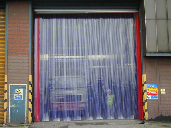
strip-doorsThe students are still there, as is the nightclub. The property in between is still there, but this time we have replaced the brick wall at the front with one of those sets of PVC strip curtains that you sometimes find covering the doors of factories, or butchers shops to keep insects out (or even lining the edge of the cold aisle in a data centre). Inside, we’ll put some comfy chairs and maybe a beer fridge. This is now our floating gate party room and the PVC strips are our thinner section of oxide layer.

Excited students going to a nightclub are stimulated so that some fall into the "Floating Gate" room

Excited students going to a nightclub are stimulated so that some fall into the “Floating Gate” room

As we now play the music loud enough to exceed the threshold, the excited students will run up the road towards the bar as before, but this time – with enough excitement – some of them will pass through the divider into our floating gate room and remain there, thus trapping electrons (sorry, I mean students) on the floating gate. Meanwhile, as the floating gate room fills up with people, the sound of the music becomes more muffled which slows down the flow of students in the road outside. To put it another way, the volume threshold at which stimulation will occur rises if there are students (sorry, I mean electrons) on the floating gate.

In a FGMOS, if a high charge is applied to the control gate in the same manner as with a MOSFET, electrons flowing from source to drain can get excited and “jump” through the oxide layer into the floating gate, increasing its retained charge. This is the program operation we have talked about so many times before: the floating gate is the “bucket of electrons” from my previous posts (a classic case of mixed metaphors). To erase the charge stored on the floating gate, a high voltage is applied across the source and drain while a negative voltage is applied to the control gate, causing the retained electrons to “jump” back off the floating gate (through the oxide layer). I’m putting the word “jump” in inverted commas there because it’s slightly more complicated and usually involves a process called Fowler–Nordheim tunnelling. I’ll explain everything I understand about that in the next paragraph.

[This paragraph intentionally left blank]

Yeah, it’s complicated, it involves quantum mechanics and it’s way over my head. I’m just taking it for granted that it works.

Read Operations

Now that we have methods for programming and erasing we just need a way of testing the value stored: a read operation. When we were talking about the MOSFET in the previous section we could control the flow of charge (which I had better start calling current) between source and drain by varying the voltage applied to the gate.

FGMOS Read Thresholds: The voltage threshold at which current begins to flow from drain to source is different depending on the charge stored on the floating gate. By testing at an intermediate reference voltage (VtREF) called the "read point" we can determine whether the floating gate contains charge (which we call ZERO) or not (which we call ONE)

FGMOS Read Thresholds: The voltage threshold at which current begins to flow from drain to source is different depending on the charge stored on the floating gate. By testing at an intermediate reference voltage (VtREF) called the “read point” we can determine whether the floating gate contains charge (which we call ZERO) or not (which we call ONE)

In the FGMOS this can be turned around so that by measuring the current we can determine the voltage on the floating gate, because electrons trapped on the floating gate cause the threshold we’ve previously mentioned to move. By applying a certain voltage (VtREF in the diagram on the right) across the source and drain and then testing the current we can determine if the voltage on the gate is above or below a specific point, called the read point.

So, if we play music at a certain threshold volume when the floating gate party room is empty, the sound travels far enough to stimulate a flow of students to the nightclub. But if the room is full (the floating gate contains charge) this specific volume will not stimulate a flow. Instead, it will require a louder threshold volume to get the students out of bed. And I think it’s time to abandon the student analogy now… let us never speak of it again.

Read Points for SLC and MLC

Read Points for SLC and MLC (image courtesy AnandTech)

If you remember, flash comes in different forms: SLC, MLC and TLC. So why are MLC reads slower than SLC, with TLC even slower still? Well, because SLC contains only one bit of data (two possible states: a zero or one), we only need to test one threshold voltage, i.e. SLC only has one read point. But for MLC, where there are two bits (and therefore four possible states), there are three read points… while for TLC there are even more.

Remember the bucket full of electrons analogy? When you test the SLC bucket to see if it’s above or below 50% full, the answer will tell you whether the stored value is a zero or a one. But for the MLC bucket, the answer to that test isn’t enough: based on the first answer you then need to perform a second test to see if the bucket is above or below 25% / 75% [delete as appropriate] full. All this additional testing takes time, which is why SLC reads are faster than MLC reads, which in turn are faster than TLC reads.

But what about the wear?

Flash Wear

broken-blindsFinally I’m getting to the point. Remember the PVC strip curtains, like the ones in the main picture at the top of this post? What do you think happens to them as all those excited students (sorry) hurtle through them? They get damaged. In a FGMOS the oxide layer which isolates the floating gate from the silicon substrate is designed to be thin enough to allow quantum tunnelling of electrons when a high enough charge is applied, but this process gradually damages the layer. Reads are not a problem because only lower voltages are used and no electron tunnelling takes place. But program and erase operations are a different story, which is why wear is measured by the number of program/erase cycles. As the layer gets more damaged, the isolation of the floating gate is increasingly affected and the probability of stored charge leaking out will increase.

For SLC this is less of an issue, because during a read we only need to measure at one read point – so there is a lot of room for error either side of the threshold. But for MLC, with three read points, we need to be much more exact. Thus the wear caused by using SLC, MLC and TLC isn’t really very different, it’s simply that the tolerances for error are much finer with the increased bit counts of MLC and TLC.

At some point, the oxide layer for a FGMOS will become sufficiently degraded so that it can no longer store charge properly on the floating gate. We won’t know about this until it happens, but at some point a read from the cell will no longer be trustworthy. And clearly that’s a problem for data storage, which is why (just like disk) flash stores error correction codes (ECC) alongside user data to ensure that incorrect information is spotted and dealt with while any underlying pages are marked as unusable – all without impacting users.

Comparison of SLC, MLC and EMLC (courtesy of EE Times)

Comparison of SLC, MLC and EMLC (courtesy of EE Times)

A final point to consider is that there is a (more expensive) form of MLC known as eMLC (the e stands for enterprise, with “normal” MLC then sometimes referred to as consumer or cMLC). The only difference between eMLC and the standard cMLC we have discussed in the past is that program and erase operations are “slowed down” for eMLC in order to cause less damage to the oxide layer. This gives slightly reduced performance but also significantly reduces wear, allowing up to 10x more P/E cycles. Opinion is divided on whether this is actually a worthwhile investment (not for me though, I think it’s a waste of money in the majority of cases).

Hot News

That’s the end of this post – and as usual I’ve committed two of my three regular blogging sins: writing too much, using silly analogies and finishing on a terrible pun. Time to complete the trio:

Some flash companies have been experimenting with methods of refreshing the lifetime of flash, with one avenue of exploration focussed on providing a short burst of heat to repair the damage to the oxide layer. It has been claimed that flash treated this way can sustain over 100 million P/E cycles with no noticeable degradation. If that is really the case – and this technology can be put into production – we might finally find that the Talking Heads were correct: in the world of flash memory we are on the road to no-wear…